 Aug 20, 2012
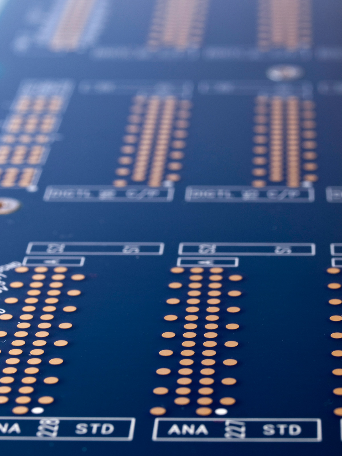
Multitest, a designer and manufacturer of final test handlers, contactors and load boards used by integrated device manufacturers (IDMs) and final test subcontractors worldwide, announces that its Pulse Plating Process provides significant advantages in terms of fabrication cost and cycle time. Multitest Pulse Plating has been released to manufacturing for all major board customers. The proprietary Multitest process has proven market-leading performance in various customer applications.
Originally the process was developed to support ultra high aspect ratio requirements at 0.4 mm pitch. Multitest has developed a customized plating process for small via diameters in high layer count PCBs used in ATE test. The process allows for .0051" diameter through-holes into PCBs with up to 40 layers.
The Multitest Pulse Plating Process is applied particularly to BGA and WLCSPs but also can be used for vertical probe applications. It eliminates the need for sequential lamination in most 0.4 mm pitch applications. This same technology is deployed for 0.3 mm pitch BGA applications with through-hole construction.
For more information, visit www.multitest.com/pcb.
Multitest (headquartered in Rosenheim, Germany) is one of the world’s leading manufacturers of test equipment for semiconductors. Multitest markets test handlers, contactors, and ATE printed circuit boards. Globally, more than 800 employees serve the company’s customers in offices and branches in North America, Singapore, Malaysia, the Philippines, Taiwan, China and Thailand. For more information, visit www.multitest.com.


.gif)

