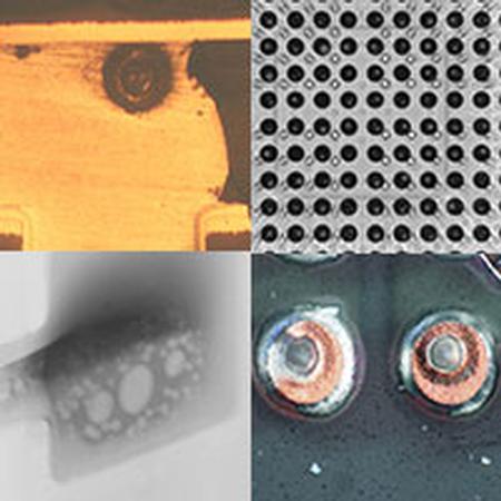
Voiding in solder joints is not new we have experienced cavities in solder joints during the introduction of through hole, surface mount and more recently area array technology. In many cases we never knew we have had voids till the introduction of x-ray inspection.
Book your place http://www.bobwillisonline.com/training_detail.asp?WorkshopID=127
Voids can be created in solder joints; your speaker once had the job of creating voids to order in solder joint of a known size. Voids can be seen in passive chip, J lead and gull wing and castellation terminations and we will show you how. Concerns were not really shown until area array technology started to increase in volume. Regardless of reliability voids or cavities on area array and large power devices will increase standoff, tilt devices and can mask other process issues.
This session will examine and demonstrate all of the common reasons why voids can form in solder joints. It will also highlight all of the inspection criterial in existing international standards.
Causes of void formation
Solder Paste volume
Via holes in mounting pads
PCB surface finish, outgassing
Component plating outgassing
Normal reaction from solder process
Non wetting or surface dewetting
Stencil design
Solder paste
Temperature profile
Component footprint
In his presentation Bob will highlight test methods you can try and tricks of the trade to understand void formation and suggestions on how to eliminate many of the common causes. After the webinar there is a Q&A session which provides ample time for all delegate questions to be answered. However if a delegate has a process example they would like cover in the webinar it will need to be provided in advance of the session. A copy of the slides is sent to each delegate after the webinar
Book your place http://www.bobwillisonline.com/training_detail.asp?WorkshopID=127


