Industry News | 2003-04-17 11:32:31.0
Taking place Sept. 28-Oct. 2, at the Minneapolis Convention Center in Minneapolis, Minn.
Industry News | 2018-12-08 03:29:29.0
SMT Dictionary – Surface Mount Technology Acronym and Abbreviation
Industry News | 2018-10-18 08:59:34.0
PRINCIPLE OF SURFACE MOUNT PROCESS(SMT PROCESS)
Industry Directory | Manufacturer
FP Stencil Sdn. Bhd. is principally involved in the manufacture and sale of laser-cut metal surface- mount technology (SMT) stencils. Our products comprise of PCB stencils, wafer stencils, mini stencils, & accessories.
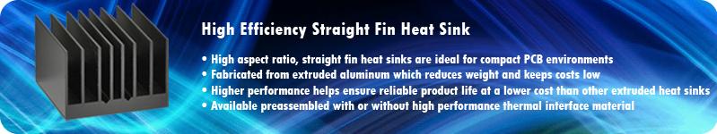
Straight Fin BGA Heat Sink (High Aspect Ratio Ext.) High aspect ratio, straight fin heat sinks that are ideal for compact PCB environments Fabricated from extruded aluminum, which minimizes thermal resistance from the base to the fins, reduc
Technical Library | 2013-03-07 18:25:36.0
The market for high-layer-count printed circuit boards (PCB) containing blind and buried vias was once relatively small, and focused on specialized applications in the military and high end computing. The demand for these types of PCBs today is being driven by an increasing number of commercial applications in the telecommunications and semiconductor test market segments. These applications typically require high-aspect-ratio plated-through-holes (PTHs) and blind and buried vias in order to meet the applications interconnect density requirements. Blind and buried vias and high aspect ratio PTHs continue to present manufacturing challenges and frequently are the limiting features to achieving high fabrication yield... First published in the 2012 IPC APEX EXPO technical conference proceedings
Technical Library | 2018-10-31 20:35:49.0
The electronics industry has grown immensely over the last few decades owing to the rapid growth of consumer electronics in the modern world. New formulations are essential to fit the needs of manufacturing printed circuit boards and semiconductors. Copper electrolytes for high throwing power applications with high thermal reliability and high throughput are becoming extremely important for manufacturing high aspect ratio circuit boards.Here we discuss innovative DC copper metallization formulations for hoist lines and VCP (Vertical Continues Plating) applications with high thermal reliability and throughput for high aspect ratio PCB manufacturing
Technical Library | 2020-07-15 18:29:34.0
In the early 2000s the first fine-pitch ball grid array devices became popular with designers looking to pack as much horsepower into as small a space as possible. "Smaller is better" became the rule and with that the mechanical drilling world became severely impacted by available drill bit sizes, aspect ratios, and plating methodologies. First of all, the diameter of the drill needed to be in the 0.006" or smaller range due to the reduction of pad size and spacing pitch. Secondly, the aspect ratio (depth to diameter) became limited by drill flute length, positional accuracy, rigidity of the tools (to prevent breakage), and the throwing power of acid copper plating systems. And lastly, the plating needed to close up the hole as much as possible, which led to problems with voiding, incomplete fill, and gas/solution entrapment.
Industry Directory | Manufacturer
A printed circuit board manufacturer producing high quality prototype printed circuit boards.

Slant Fin BGA Heat Sink (High Aspect Ratio Ext.) Features a low profile, slant fin array that offers many of the performance benefits of maxiFLOW™ at a great value Fabricated from extruded aluminum, which minimizes thermal resistance from th

.gif)


