New Equipment | Assembly Services
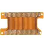
TW-FPC--Flexible PCB 0187 Price: Get Latest Price Minimum Order Quantity: 10 Unit/Units other Port: HK Packaging Details: blister and package Delivery Time: 1 week Payment Terms: L/C,D/P,T/T,Western Union Supply Ability: 5000000 Unit/Units p
Technical Library | 2020-09-02 22:02:13.0
With the adoption of Wafer Level Packages (WLP) in the latest generation mobile handsets, the Printed Circuit Board (PCB) industry has also seen the initial steps of High Density Interconnect (HDI) products migrating away from the current subtractive processes towards a more technically adept technique, based on an advanced modified Semi Additive Process (amSAP). This pattern plate process enables line and space features in the region of 20um to be produced, in combination with fully filled, laser formed microvias. However, in order to achieve these process demands, a step change in the performance of the chemical processes used for metallization of the microvia is essential. In the electroless Copper process, the critical activator step often risks cross contamination by the preceding chemistries. Such events can lead to uncontrolled buildup of Palladium rich residues on the panel surface, which can subsequently inhibit etching and lead to short circuits between the final traces. In addition, with more demands being placed on the microvia, the need for a high uniformity Copper layer has become paramount, unfortunately, as microvia shape is often far from ideal, the deposition or "throw" characteristics of the Copper bath itself are also of critical importance. This "high throwing power" is influential elsewhere in the amSAP technique, as it leads to a thinner surface Copper layer, which aids the etching process and enables the ultra-fine features being demanded by today's high end PCB applications. This paper discusses the performance of an electroless Copper plating process that has been developed to satisfy the needs of challenging amSAP applications. Through the use of a radical predip chemistry, the formation, build up and deposition of uncontrolled Pd residues arising from activator contamination has been virtually eradicated. With the adoption of a high throwing power Copper bath, sub 30um features are enabled and microvia coverage is shown to be greatly improved, even in complex via shapes which would otherwise suffer from uneven coverage and risk premature failure in service. Through a mixture of development and production data, this paper aims to highlight the benefits and robust performance of the new electroless Copper process for amSAP applications
Industry News | 2010-04-09 21:17:21.0
Five of Indium Corporation's technology experts will present their technical findings at APEX in Las Vegas, Nevada, April 6-9, 2010.
Industry News | 2023-05-22 18:45:34.0
SHENMAO America, Inc. is proud to announce the release of its new SMBF-08 Visible No-Clean BGA Flux. This innovative flux is specifically designed to meet the demands of surface mount technology (SMT) assembly and BGA ball mount processes, offering enhanced visibility and performance.
Industry News | 2010-09-28 10:51:42.0
Kyzen, a world leading provider of environmentally responsible precision cleaning products for electronics and high-technology manufacturing operations, announces that Rich Brooks will present a paper titled “Issues and Concerns in Cleaning Under Low Profile Components” at the upcoming SMTA International, scheduled to take place October 25-28, 2010 at the Walt Disney World Swan and Dolphin Resort in Orlando, FL.
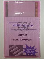
SIPAD Solid Solder Deposit (ssd) is a Siemens patented process that pre loads the pc board surface mount pads with solder in a solid form. Boards are printed, reflowed without components producing a predictable repeatable meniscus. SIPAD boards a
New Equipment | Fabrication Services
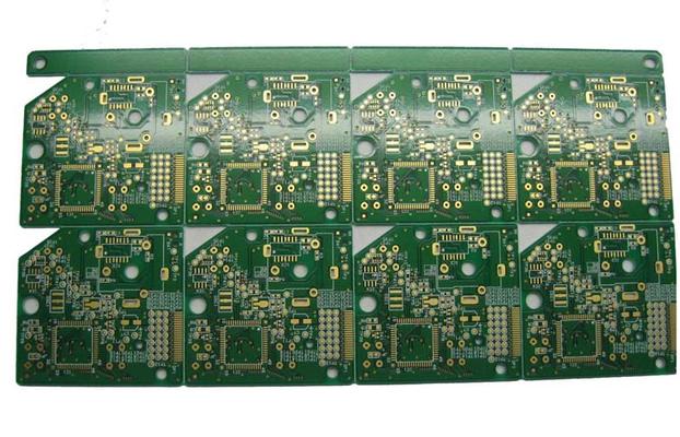
Low Cost Heavy Copper PCB China 4 Layers Circuit Boards Supplier Quick Details: FR4 base material 1.6mm board thickness 2oz heavy copper Plating gold finishing RF custom PCB boards Used for Radio Frequency From China PCB manufacturer Specifications

Innovative Materials, Superior Performance. Our printed circuit board and semiconductor packaging materials provide superior thermal and mechanical performance, a fact we’ve prided ourselves on for over 45 years. All our materials are RoHS complian
New Equipment | Solder Materials
Indium Corporation manufactures high quality solder powders and pastes. Powders are available in hundreds of alloys and a full range of sizes. Solder pastes can be made from these powders using a wide variety of flux vehicles to get the best fit for
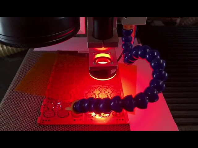
355nm 10W /15W High-Precision CCD FPC/PCB UV Laser Cutting Machine With Perfect CAM interface, it supports the mainstream of the drilling and milling file format; man-machine interface is friendly; optical path is sealed, and it also has stable an


