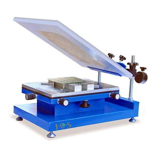
Application: MSP-250 series is suitable for mobile phone motherboard, computer motherboards, single and double side PCB, LED display circuit boards, LED light bar, FPC board, etc. Acceptable Printing Materials: Ink, solder paste, red glue, silver pa
Industry Directory | Manufacturer
a pcb manufacturer in China specializing in multi-layer pcbs that meet RoHs, UL, IPC standards.
Industry Directory | Manufacturer's Representative
Camtech Circuits is ISO9001:2008 and UL certificated. We strictly implement ISO9001 quality management system. Each equipment, every process has its own Manual of Engineering Instructions. No matter p
Industry Directory | Manufacturer
Since 1971, Eagle Electronics Inc. has provided our Customers with the highest quality Printed Circuit Boards at fair and competitive prices.
Technical Library | 2021-11-03 17:05:39.0
Additively printed circuits provide advantages in reduced waste, rapid prototyping, and versatile flexible substrate choices relative to conventional circuit printing. Copper (Cu) based inks along with intense pulsed light (IPL) sintering can be used in additive circuit printing. However, IPL sintered Cu typically suffer from poor solderability due to high roughness and porosity. To address this, hybrid Cu ink which consists of Cu precursor/nanoparticle was formulated to seed Cu species and fill voids in the sintered structure. Nickel (Ni) electroplating was utilized to further improve surface solderability. Simulations were performed at various electroplating conditions and Cu cathode surface roughness using the multi-physics finite element method. By utilizing a mask during IPL sintering, conductivity was induced in exposed regions; this was utilized to achieve selective Ni-electroplating. Surface morphology and cross section analysis of the electrodes were observed through scanning electron microscopy and a 3D optical profilometer. Energy dispersive X-ray spectroscopy analysis was conducted to investigate changes in surface compositions. ASTM D3359 adhesion testing was performed to examine the adhesion between the electrode and substrate. Solder-electrode shear tests were investigated with a tensile tester to observe the shear strength between solder and electrodes. By utilizing Cu precursors and novel multifaceted approach of IPL sintering, a robust and solderable Ni electroplated conductive Cu printed electrode was achieved.
4 hours Thin Film Set Time (.001" @ 25°C) >12 hours Total % NV Solids 100% Hegman Gauge Volume Resi
New Equipment | Cleaning Equipment
Features ● Equipment is ergonomically in designed. ● Auto liquid feeding and draining system. ● Five levels filter system,liquid can be recycled which results in lower solvent consumption. ● Internationally recognized critical components are used to
Industry News | 2011-11-08 13:28:32.0
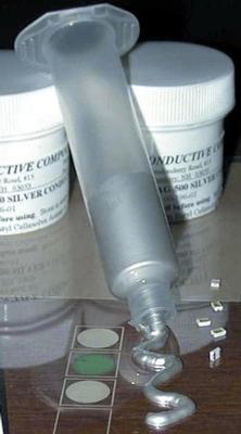
Engineered Conductive Materials introduces its DB-1588 low-cost conductive adhesive for back contact applications in crystalline silicon solar modules.
Technical Library | 2017-11-22 12:38:51.0
The use of copper foils laminated to polyimide (PI) as flexible printed circuit board precursor is a standard practice in the PCB industry. We have previously described[1] an approach to very thin copper laminates of coating uniform layers of nano copper inks and converting them into conductive foils via photonic sintering with a multibulb conveyor system, which is consistent with roll-to-roll manufacturing. The copper thickness of these foils can be augmented by electroplating. Very thin copper layers enable etching fine lines in the flexible circuit. These films must adhere tenaciously to the polyimide substrate.In this paper, we investigate the factors which improve and inhibit adhesion. It was found that the ink composition, photonic sintering conditions, substrate pretreatment, and the inclusion of layers (metal and organic) intermediate between the copper and the polyimide are important.
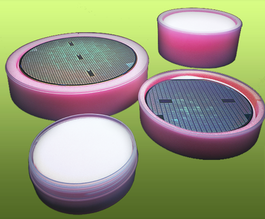
Silicon wafer-level packaging systems for storing and shipping integrated circuits for the semiconductor industry for 75mm 100mm 150mm 200mm 300mm and even square solar solutions. Plastic packaging jars antistatic and conductive foam liners cushions,


