
Used SMT Equipment | Soldering - Reflow
TrioTek: Ultraviolet UV Curing, IR Thermal Curing, Moisture Curing for encapsulants, adhesives, conformal coatings and potting compounds TrioTek™ inline curing ovens from ETS are ideal for medium to high-volume curing or drying of encapsulants, con

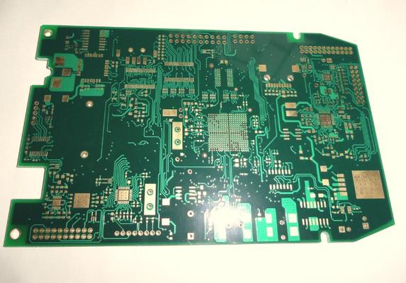
Layer: 8 layers Material: FR-4 Board Thickness: 0.6mm Surface Finish: Immersion Gold 1~4u Copper Thickness: 1/3 oz Impedance, 4/4mils width/spacing Layers: 2--36layers Max manufacturing size: 640mm*1100mm Copper foil thickness: 0.5OZ-13OZ M

Layer: 2 Material: FR-4 Board Thickness: 1.6mm Surface Finish: HAL Copper Thickness: 2/2 oz Green Solder Mask Layers: 2--36layers Max manufacturing size: 640mm*1100mm Copper foil thickness: 0.5OZ-13OZ Min line width/space: 3mil/3mil Min
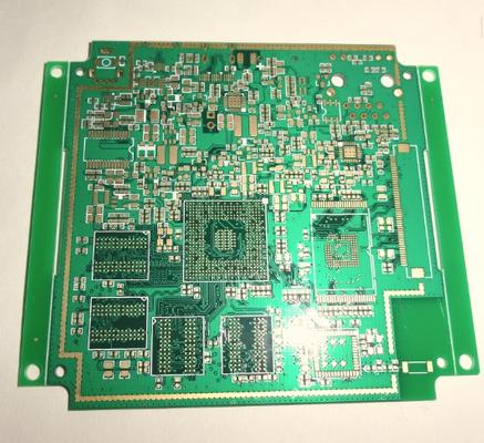
Layer: 6 layers Material: FR-4 Board Thickness: 1.0mm Surface Finish:ENIG Copper Thickness: 1 oz all layers Blind via L1~L2 and L1~L3 Layers: 2--36layers Max manufacturing size: 640mm*1100mm Copper foil thickness: 0.5OZ-13OZ Min line width
500⁰C) Compatible with multiple lamination cycles Standard PCB lamination cycles may be used Excellent for Laser Via formation Excellent CAF resistance Uses standard desmear and plating processes High Modulus: 1100 kpsi Lo
New Equipment | Solder Paste Stencils
Through the increase of mixed technologies, stepped stencils have gained importance to the electronic assembly manufacturer. If the solder paste quantity can no longer be adequately regulated by adjusting Step/Relief Stencil Picture the pad sizes, st
Industry News | 2018-10-18 11:08:03.0
Different Techniques for Plating
Technical Library | 2019-02-13 13:45:11.0
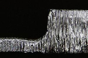
Development of information and telecommunications network is outstanding in recent years, and it is required for the related equipment such as communication base stations, servers and routers, to process huge amount of data in no time. As an electrical signal becomes faster and faster, how to prevent signal delay by transmission loss is a big issue for Printed Circuit Boards (PCB) loaded on such equipments. There are two main factors as the cause of transmission loss; dielectric loss and conductor loss. To decrease the dielectric loss, materials having low dielectric constant and low loss tangent have been developed. On the other hand, reducing the surface roughness of the copper foil itself to be used or minimizing the surface roughness by modifying surface treatment process of the conductor patterns before lamination is considered to be effective in order to decrease the conductor loss. However, there is a possibility that reduction in the surface roughness of the conductor patterns will lead to the decrease in adhesion of conductor patterns to dielectric resin and result in the deterioration of reliability of PCB itself. In this paper, we will show the evaluation results of adhesion performance and electrical properties using certain type of dielectric material for high frequency PCB, several types of copper foil and several surface treatment processes of the conductor patterns. Moreover, we will indicate a technique from the aspect of surface treatment process in order to ensure reliability and, at the same time, to prevent signal delay at the signal frequency over 20 GHz.
Technical Library | 2024-06-23 21:57:16.0
Two extremes of reflow time scale for copper pillar flip chip solder joints were explored in this study. Sn-2.5Ag solder capped pillars were joined to laminate substrates using either conventional forced convection reflow or the controlled impingement of a defocused infrared laser. The laser reflow joining process was accomplished with an order of magnitude reduction in time above liquidus and a similar increase in solidification cooling rate. The brief reflow time and rapid cooling of a laser impingement reflow necessarily affects all time and temperature dependent phenomena characteristic of reflowed molten solder. These include second phase precipitate dissolution, base metal (copper) dissolution, and the extent of surface wetting. This study examines the reflow dependent microstructural aspects of flip chip Sn-Ag joints on samples of two different size scales, the first with copper pillars of 70μm diameter on 120μm pitch and the second with 23μm diameter pillars on a 40μm pitch. The length scale of Pb-free solder joints is known to affect the Sn grain solidification structure; Sn grain morphology will be noted across both reflow time and joint length scales. Sn grain morphology was further found to be dependent on the extent of surface wetting when such wetting circumvented the copper diffusion barrier layer. Microstructural analysis also will include a comparison of intermetallic structures formed; including the size and number density of second phase Ag3Sn precipitates in the joint and the morphology and thickness of the interfacial intermetallics formed on the pillar and substrate surfaces.


