Industry News | 2011-04-20 21:26:17.0
IPC — Association Connecting Electronics Industries® presented Special Recognition, Distinguished Committee Leadership and Committee Service awards and a Presidents Award at IPC APEX EXPO™, held April 10–14, in Las Vegas.
Industry News | 2014-03-28 09:54:48.0
IPC – Association Connecting Electronics Industries® presented Committee Leadership, Distinguished Committee Service and Special Recognition Awards at IPC APEX EXPO® at Mandalay Bay Convention Center in Las Vegas.
New Equipment | Test Equipment
The Calotest provides quick, simple and inexpensive determination of coating thickness. A sphere of a known diameter is rotated against the coating surface and the addition of an abrasive slurry causes a spherically-shaped depression to be abraded th
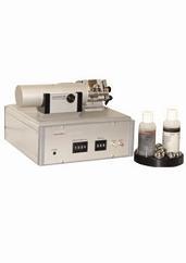
New Equipment | Test Equipment
The CALOTEST® is widely used for analyzing coatings with thicknesses of between 0.1 and 50 µm. The simple ball-cratering method is a fast and accurate means of checking the thickness of any coating, whether a single or multilayered stack. Typical exa
Technical Library | 2013-01-03 20:27:54.0
Electronics assemblies with large flip-chip BGA packages can be prone to either pad cratering or brittle intermetallic (IMC) failures under excessive PCB bending. Pad cratering cracks are not detected by electrical testing or non-destructive inspection methods, yet they pose a long term reliability risk since the cracks may propagate under subsequent loads to cause electrical failure. Since the initiation of pad cratering does not result in an instantaneous electrical signature, detecting the onset of this failure has been challenging. An acoustic emission methodology was recently developed by the authors to detect the onset of pad cratering. The instantaneous release of elastic energy associated with the initiation of an internal crack, i.e., Acoustic Emission (AE), can be monitored to accurately determine the onset of both pad cratering and brittle intermetallic (IMC) failures.
Technical Library | 2015-08-13 15:52:40.0
Pad cratering has become more prevalent with the switch to lead free solders and lead free compatible laminates. This mainly is due to the use of higher reflow temperature, stiffer Pb-free solder alloys, and the more brittle Pb-free compatible laminates. However, pad cratering is difficult to detect by monitoring electric resistance since pad cratering initiates before an electrical failure occurs. Several methods have been developed to evaluate laminate materials' resistance to pad cratering. Pad-solder level tests include ball shear, ball pull and pin pull. The detailed methods for ball shear, ball pull, and pin pull testing are documented in an industry standard IPC-9708. Bansal, et al. proposed to use acoustic emission (AE) sensors to detect pad cratering during four-point bend test. Currently there is an industry-working group working on test guidelines for acoustic emission measurement during mechanical testing.
Technical Library | 2012-09-06 18:19:37.0
First published in the 2012 IPC APEX EXPO technical conference proceedings. Pad Cratering opens circuits. This occurs when the resin crack (fracture) migrates through a copper trace or via. This happens at assembly, in service or during handling. When com
Technical Library | 2019-05-08 21:52:28.0
Cold ball pull testing is used to validate the resistance of PCB pad cratering for the different ultra-low loss dielectrics materials (Dk=3~4.2 and Df
Technical Library | 2015-02-19 16:54:34.0
Pad cratering is an important failure mode besides crack of solder joint as it’ll pass the regular test but have impact on the long term reliability of the product. A new pin pull test method with solder ball attached and positioning the test board at an angle of 30º is employed to study the strength of pad cratering. This new method clearly reveals the failure mechanism. And a proper way to interpret the finite element analysis (FEA) result is discussed. Impact of pad dimension, width and angle of copper trace on the strength is included. Some findings not included in previous research could help to guide the design for better performance
Technical Library | 2015-10-29 18:19:33.0
With the electronic industry moving towards lead-free assembly, traditional SnPb-compatible laminates need to be replaced with lead-free compatible laminates that can withstand the higher reflow temperature required by lead-free solders. Lead-free compatible laminates with improved heat resistance have been developed to meet this challenge but they are typically more brittle than SnPb laminates causing some to be more susceptible to pad cratering. In this paper, two novel approaches for minimizing pad cratering will be discussed. Preliminary results which validate the two approaches will also be presented.


