New Equipment | Test Equipment
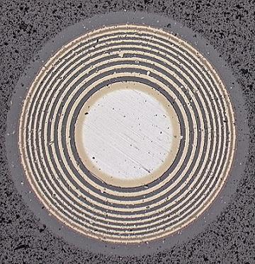
The Calotest provides quick, simple and inexpensive determination of coating thickness. A sphere of a known diameter is rotated against the coating surface and the addition of an abrasive slurry causes a spherically-shaped depression to be abraded th
New Equipment | Test Equipment
The CALOTEST® is widely used for analyzing coatings with thicknesses of between 0.1 and 50 µm. The simple ball-cratering method is a fast and accurate means of checking the thickness of any coating, whether a single or multilayered stack. Typical exa
Electronics Forum | Wed Jul 01 13:17:39 EDT 2015 | davef
Cheryl Tulkoff and Randy Schueller do a good job summarizing the thinks on pad cratering here: http://www.smta.org/chapters/files/uppermidwest_padcratering.pdf Potential Mitigations to Pad Cratering * Board Redesign * Solder mask defined vs. non-s
Electronics Forum | Wed Jul 01 04:54:28 EDT 2015 | jvercamm
hi, the last post on pad cratering dates from 2012. We have (likely similar) problems with a RoHS 783 solder ball BGA size 29x29mm^2 (organic package BT), pitch is 1mm and solder ball diam is 0.5mm the field failure is after 12 months, almost exclu
Industry News | 2011-03-31 11:54:23.0
Over the past few years, pad cratering has become a vexing problem in lead-free assemblies, largely attributed to problems with the resin used to make a printed board. To help industry eliminate the defect and, at the same time, cut costs, IPC — Association Connecting Electronics Industries® has released IPC-9708, Test Methods for Characterization of PCB Pad Cratering.
Industry News | 2012-03-14 12:30:54.0
The SMTA is pleased to announce several new online presentations coming up this Spring. Webtorials are two-part (90 minutes each part) online presentations that provide more depth on a subject and are comparable to half-day tutorials.
Technical Library | 2013-01-03 20:27:54.0
Electronics assemblies with large flip-chip BGA packages can be prone to either pad cratering or brittle intermetallic (IMC) failures under excessive PCB bending. Pad cratering cracks are not detected by electrical testing or non-destructive inspection methods, yet they pose a long term reliability risk since the cracks may propagate under subsequent loads to cause electrical failure. Since the initiation of pad cratering does not result in an instantaneous electrical signature, detecting the onset of this failure has been challenging. An acoustic emission methodology was recently developed by the authors to detect the onset of pad cratering. The instantaneous release of elastic energy associated with the initiation of an internal crack, i.e., Acoustic Emission (AE), can be monitored to accurately determine the onset of both pad cratering and brittle intermetallic (IMC) failures.
Technical Library | 2015-08-13 15:52:40.0
Pad cratering has become more prevalent with the switch to lead free solders and lead free compatible laminates. This mainly is due to the use of higher reflow temperature, stiffer Pb-free solder alloys, and the more brittle Pb-free compatible laminates. However, pad cratering is difficult to detect by monitoring electric resistance since pad cratering initiates before an electrical failure occurs. Several methods have been developed to evaluate laminate materials' resistance to pad cratering. Pad-solder level tests include ball shear, ball pull and pin pull. The detailed methods for ball shear, ball pull, and pin pull testing are documented in an industry standard IPC-9708. Bansal, et al. proposed to use acoustic emission (AE) sensors to detect pad cratering during four-point bend test. Currently there is an industry-working group working on test guidelines for acoustic emission measurement during mechanical testing.

ACI Technologies Inc. (ACI) is a scientific research corporation dedicated to the advancement of electronics manufacturing processes and materials for The Department of Defense and industry. This video provides an overview of our commercial service
Events Calendar | Thu Oct 03 00:00:00 EDT 2019 - Thu Oct 03 00:00:00 EDT 2019 | ,
IPC Tech Ed Webinar Series: Ball Grid Array (BGA) and Bottom Termination Component (BTC) Design and Assembly Challenges: Reflow Profiling to Achieve Low Defect Rates and Successful Assembly! – Part 2
Events Calendar | Mon Apr 23 00:00:00 EDT 2018 - Thu Apr 26 00:00:00 EDT 2018 | Shanghai, China
SMTA China East Conference 2018
SMTnet Express, August 13, 2015, Subscribers: 23,186, Members: Companies: 14,558 , Users: 38,745 Pad Cratering Susceptibility Testing with Acoustic Emission Wong Boon San, Julie Silk; Agilent Technologies | Richard Nordstrom, Ph.D.; Acoustic
Investigation of Pad Cratering in Large Flip-Chip BGA using Acoustic Emission SMTnet Express January 3, 2013, Subscribers: 26072, Members: Companies: 9076, Users: 34113 Investigation of Pad Cratering in Large Flip-Chip BGA using Acoustic Emission
| https://www.eptac.com/wp-content/uploads/2013/08/eptac_08_21_13-1.pdf
Surface Mount Technology Association (SMTA) | https://www.smta.org/smtai/call_for_papers.cfm
& Solderability Pad Cratering Soldermask Substrate Reliability Process Control: Acoustic Imaging (C-SAM) Bene-ts of AOI & SPI CIM In-Circuit Test Process Modeling Software Test Strategies 2D/3D X-Ray Thanks and the SMTAI Technical Committee looks forward to hearing from you


.gif)
winsouce.jpg)