Technical Library | 2023-01-17 17:29:40.0
A Practical Investigation into the Use of No Lead Solders for SMT Reflow
Technical Library | 2020-01-28 00:23:58.0
This paper explores new advances in the reflow soldering process including vacuum technology and warpage mitigation systems. The first topic for discussion will be the implementation of a vacuum process directly in a conventional inline soldering system. The second topic presented is the mitigation of warpage on substrates or wafers.
Technical Library | 2023-01-17 17:37:45.0
Various international market trends drive electronics manufacturers and their mate- rials and equipment suppliers to develop new assembly techniques to reduce the industry's environmental impact. Two pri- mary forces in this drive are the movements to lead-free assembly and ISO 14000 cer- tification. In response to these factors, reflow technology advances are enabling manufacturers to meet or anticipate the new environmental mandates.
i4.0 Today caught up with Marc Peo of Heller Industries at IPC Apex Expo in San Diego, to discuss the IPC CFX initiative. Check out the rest of the CFX Videos from IPC APEX EXPO 2018 here: CFX Highlights: https://youtu.be/Q7_fWK7_zeA IPC Representati
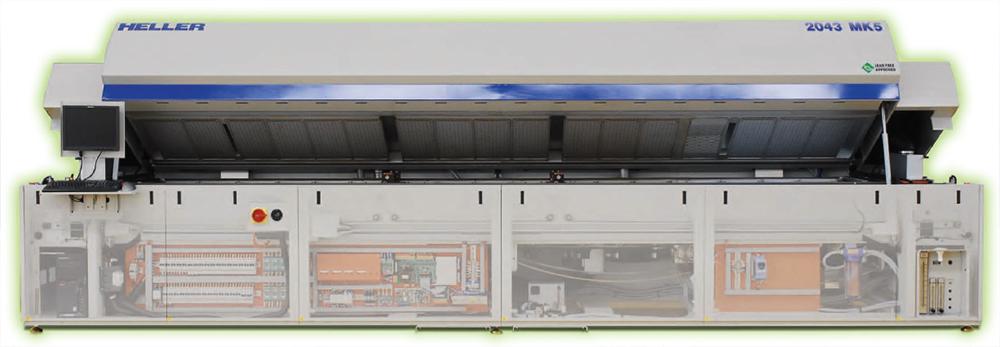
The World's Best Convection Reflow Oven The ultimate high volume production reflow oven with belt speeds up to 1.4 m/min to accommodate the fastest pick and place systems. Lead Free Certified reflow oven! Maintenance Free! Lowest Nitrogen &
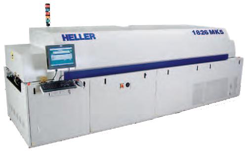
The World's Best SMT Convection Reflow Ovens for Large Boards and Dual Lane 1826 Mark 5 reflow oven provides consistent performance for high volume reflow requirements while minimizing preventative maintenance and floorspace. Lead Free Certified!
Technical Library | 2023-01-17 17:50:59.0
Heller's new Condenser Tube Flux Recovery System is designed to provide more efficient flux collection than earlier Heller flux collection systems; while providing minimal down time for inspection and cleaning. The entire system easily fits within the rear of the top shell of an 1800-EXL oven. The system utilizes a different set of top shell caps specially designed to provide the best serviceability of both the flux collection system and maintenance of the heater zone blower motors.
Nano-copper sintering in formic acid vapor.
Increase productivity, improve quality, reduce costs with vertical format curing solutions from Heller Industries. Learn more: http://www.hellerindustries.com/755-Vertical-Oven.php
Technical Library | 2019-07-10 23:36:14.0
Pockets of gas, or voids, trapped in the solder interface between discrete power management devices and circuit assemblies are, unfortunately, excellent insulators, or barriers to thermal conductivity. This resistance to heat flow reduces the electrical efficiency of these devices, reducing battery life and expected functional life time of electronic assemblies. There is also a corresponding increase in current density (as the area for current conduction is reduced) that generates additional heat, further leading to performance degradation.


