Industry Directory | Manufacturer
With numerous facilities in the United States, we are one of the electronics industry's leading manufacturers of lead-free solder products, superior quality stencils, and precision cut parts.
Industry Directory | Manufacturer
We guarentee to lower your product cost! With over 15 years experience, we are DIRECT CONTACTS of select Asian manufacturing companies and factories from The People's Republic of China, Philippines, and Hong Kong. This select group is well-established manufacturing experts within their industries. We have long term relations with each
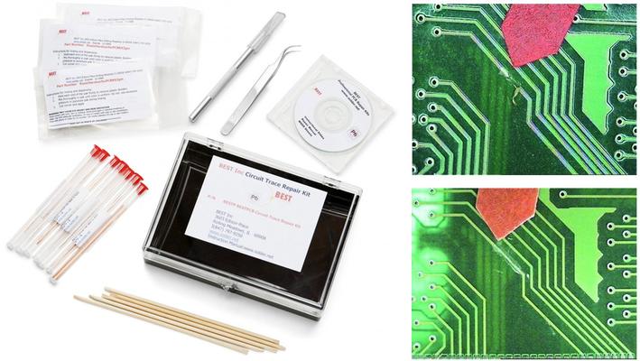
New Equipment | Rework & Repair Equipment
The BEST PCB circuit trace repair kit gives you the tools you need for fast modification and repair of PCB circuit traces. Our online PCB repair training videos, our master instructors along with these materials allows you to meet the original PCB qu

New Equipment | Fabrication Services
Multi-Layer flexible circuits consist of 3-6 copper layers encapsulated with dielectric, normally connected with a plated thru-hole (see diagram below). Multi-layer circuits can be fabricated with or without coverlayers. When to Use Multi-Layer Fle
Electronics Forum | Mon Apr 29 05:25:13 EDT 2002 | ianchan
Hi, we do Sn plated I/O pinning insertion into Ni/Au thru' holes. no problems here so far, as we cater for the "interference" (fit-allowances) of the I/O pin into the thru' diameter, via improved PCB thru' hole designs. before this cater/considerati
Electronics Forum | Fri Jun 18 12:50:32 EDT 1999 | jseagle
We currently use HASL on all of our boards and I would like to move to something else. I have sampled some boards with Entek OSP and I loved it, the problem is we have plated mounting holes on just about every board we make. Does anyone have inform
Industry News | 2018-10-18 11:08:03.0
Different Techniques for Plating
Industry News | 2018-12-08 03:29:29.0
SMT Dictionary – Surface Mount Technology Acronym and Abbreviation

PCB pad circuit repair using epoxy. Using multiple angles including overhead and from both right and left angles the BEST instructor staff demonstrates plainly how to repair a PCB pad using the epoxy method. This method is per IPC 7721 4.4.1. http://
With the development of miniaturization of assembly components, the layout area and pattern design area of PCBs have also been continuously reduced, and PCB manufacturers are constantly updating the production process to conform to the development tr
SMT Express, Issue No. 2 - from SMTnet.com Volume 1, Issue No. 2 Wednesday, July 14, 1999 Featured Article Continued From Previous Page PRINTED CIRCUIT BOARD FABRICATION BASICS AN OUTLINE Earl Moon Proof Of Design (POD) 8. PLATING (AND
| https://www.eptac.com/wp-content/uploads/2013/04/eptac_05_22_13.pdf
Imagineering, Inc. | https://www.pcbnet.com/quote/board-quote-usa/?cpn=3
0.025", smallest hole 0.015", all Plated holes, smallest trace/space 0.007", Green LPI Mask, White Top Silkscreen, Individual board with Single circuit design and No Multiple images of boards. File type: 274x required. No paint

.gif)
.gif)


