New Equipment | Wave Soldering
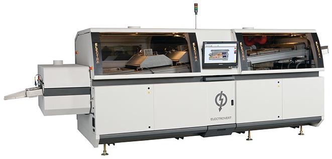
The most advanced high-performance wave soldering system designed for high-volume manufacturing. Electra's proven performance has provided the electronics assembly industry with world-class soldering results. The Electra system is designed with
New Equipment | Wave Soldering
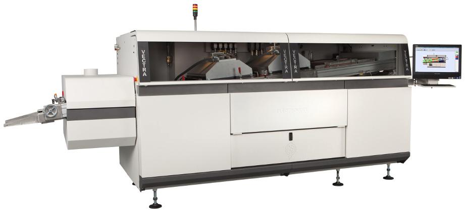
The ELECTROVERT VectraElite is the wave soldering solution for medium to high volume production that requires fast changeover, process flexibility, and system reliability. The VectraElite combines innovative technology in an accessible platform provi
New Equipment | Fabrication Services
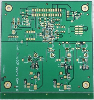
Minimum line width/space: 4mils Surface finish: immersion gold Board thickness: 1.60MM Minimum drilled hole diameter: 4mils Copper thickness: 0.5oz Special process : 0.25MM BGA , resin plugged vias in BGA pads

Parts & Supplies | Circuit Board Assembly Products
1). 80 *190mm/2up, FR-4 2). 6 layers at 1.4mm thick 3). 35 μm copper weight 4). Green solder mask LPI/White legend 5). ENIG surface finish 6). Blind via from Layer 1 to layer 2 7). Via in pad plugged conductive resin
Technical Library | 2019-10-10 00:26:28.0
Voids are a plague to our electronics and must be eliminated! Over the last few years we have studied voiding in solder joints and published three technical papers on methods to "Fill the Void." This paper is part four of this series. The focus of this work is to mitigate voids for via in pad circuit board designs. Via holes in Quad Flat No-Lead (QFN) thermal pads create voiding issues. Gasses can come out of via holes and rise into the solder joint creating voids. Solder can also flow down into the via holes creating gaps in the solder joint. One method of preventing this is via plugging. Via holes can be plugged, capped, or left open. These via plugging options were compared and contrasted to each other with respect to voiding. Another method of minimizing voiding is through solder paste stencil design. Solder paste can be printed around the via holes with gas escape routes. This prevents gasses from via holes from being trapped in the solder joint. Several stencil designs were tested and voiding performance compared and contrasted. In many cases voiding will be reduced only if a combination of mitigation strategies are used. Recommendations for combinations of via hole plugging and stencil design are given. The aim of this paper is to help the reader to "Fill the Void."
Technical Library | 2020-07-15 18:49:03.0
Via Filling • Through Hole Vias - IPC-4761 – Plugging – Filling – Filled & Capped • MicroviaFilling and Stacked Vias
Industry Directory | Manufacturer
Manufacturer of flex, rigid-flex, and rigid circuit boards. We offer prototype and production delivery options. We manufacture commercial, military, medical and industrial jobs and offer value added services such as assembly. We can customize services to fit your needs, such as gold or white tin plating, plugged or blind vias, etc.
Technical Library | 2014-11-13 19:23:50.0
With increasing power loss of electrical components, thermal performance of an assembled device becomes one of the most important quality factors in electronic packaging. Due to the rapid advances in semiconductor technology, particularly in the regime of high-power components, the temperature dependence of the long-term reliability is a critical parameter and has to be considered with highest possible care during the design phase (...) The aim of this paper is to give a short overview about standard thermal solutions like thick copper, thermal vias, plugged vias or metal core based PCBs. Furthermore, attention will be turned on the development of copper filled thermal vias in thin board constructions...
Industry News | 2010-11-09 10:15:49.0
With IPC-4761 as its guide, PCB Manufacturer sheds light on Via Plugging from the fabrication perspective.
Technical Library | 2021-05-26 00:53:26.0
This paper describes a copper electroplating enabling technology for filling microvias. Driven by the need for faster, smaller and higher performance communication and electronic devices, build-up technology incorporating microvias has emerged as a viable multilayer printed circuit manufacturing technology. Increased wiring density, reduced line widths, smaller through-holes and microvias are all attributes of these High Density Interconnect (HDI) packages. Filling the microvias with conductive material allows the use of stacked vias and via in pad designs thereby facilitating additional packaging density. Other potential design attributes include thermal management enhancement and benefits for high frequency circuitry. Electrodeposited copper can be utilized for filling microvias and provides potential advantages over alternative via plugging techniques. The features, development, scale up and results of direct current (DC) and periodic pulse reverse (PPR) acid copper via filling processes, including chemistry and equipment, are described.


