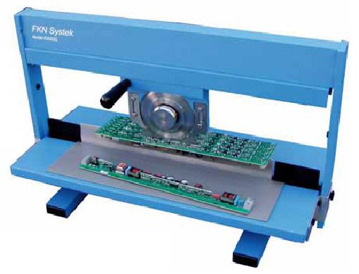
FKN Systek K3000 - Singulate scored and skip scored panels up to 24" long ESD protective mat on back table Adjustable front and back support table Singulate panels with components up to 2.5" high Available in 18" blade (standard) or 24" blade (
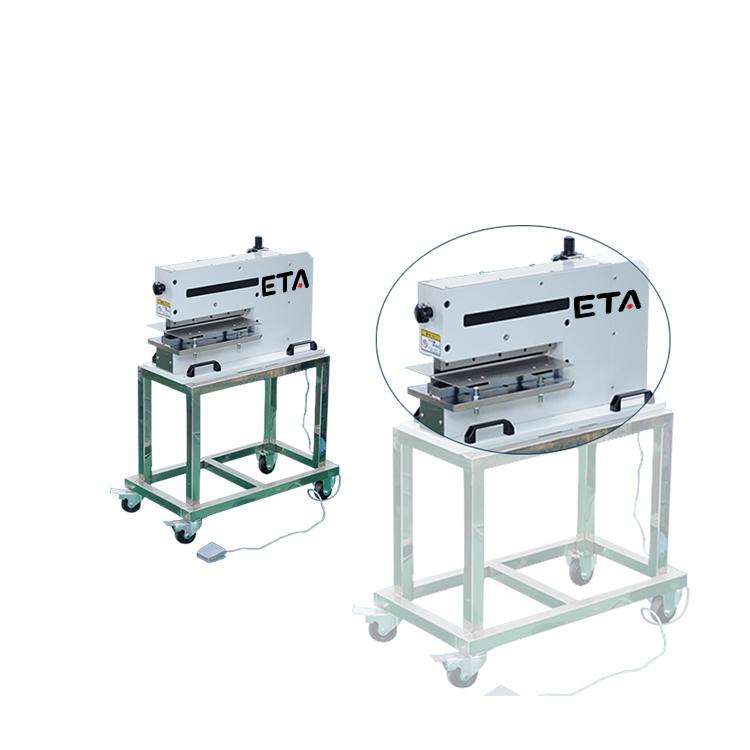
Guillotine Type PCB V-cut Machine ETA-GV330 If you could not find any similar items you want, you may send some photos to us. because our catalog and website haven't included all of our products. PCB cutting machine,PCB cutter,PCB separator,PCB
Electronics Forum | Tue Aug 15 07:02:13 EDT 2000 | George Verboven
We are assembling SMD-Leds (Chip LED cl-220yg-c-ts)on flex foil with Electrical conductive glue (Matthey A1401). When we investigated these foils we found cracks between the conductive adhesive and round the edge of the Chip-leds. This cracks cause f
Electronics Forum | Wed Jun 22 08:19:05 EDT 2005 | cyber_wolf
Our TP9 UFP machine keeps nicking the edges of A12 tool tips. I think it is because the X axis is bouncing when it comes to the component pick position. When the X bounces it is causing the tool to hit the tape hold down arm. Has anyone ever encount
Industry News | 2023-04-17 08:30:03.0
A family-owned business, Robotas Technologies has been a leader in the field of optimizing the PCB assembly process for customers all over the world for the past 35 years. The company develops lean production systems wherever people are building product, driving quality, and delivering greater productivity. Robotas' products help streamline electronics assembly, using unique features and technology to support leading OEM and EMS manufactures achieve high quality and flexible Through Hole assembly. Customers are often in the aerospace, defense and high voltage sectors who manufacture PCBs with a high percentage of odd-form components. Their latest product development reinvents clinched PCB assembly. We recently spoke with Managing Director Nick Walters to find out more about Robotas Technologies and how their technology adds value to THT assembly in PCBA.
Industry News | 2017-05-20 15:06:05.0
PCB array panelization can be a major challenge for PCB designers. Learn best practices for designing PCB boards for most efficient panelization.
Technical Library | 2016-11-17 14:58:02.0
Since 2006 RoHS requirements have required lead free solders to take the place of tin-lead solders in electronics. The problem is that in some environments the lead free solders are less reliable than the older tin-lead solders. One of the ways to solve this problem is to corner stake, edge bond or underfill the components. When considering what mitigation technique and material to use, the operating conditions must be characterized. The temperature range is important when selecting a material to use since the glass transition temperature (Tg) and coefficient of thermal expansion (CTE) are important properties. If improperly chosen, the mitigation material can cause more failures than an unmitigated component.

FKN Systek K3000 - Singulate scored and skip scored panels up to 24" long ESD protective mat on back table Adjustable front and back support table Singulate panels with components up to 2.5" high Available in 18" blade (standard) or 24" blade (
Guillotine Type PCB V-cut Machine ETA-GV330 If you could not find any similar items you want, you may send some photos to us. because our catalog and website haven't included all of our products. PCB cutting machine,PCB cutter,PCB separator,PCB
Training Courses | ONLINE | | ESD Control Training Courses
Browse training and certification programs for electrostatic discharge (ESD) control in electronics assembly.
Events Calendar | Tue Apr 13 00:00:00 EDT 2021 - Tue Apr 13 00:00:00 EDT 2021 | ,
Boston Chapter Webinar: Cleaning Chemistry For PWB and Rework - Part 2, session 1
Events Calendar | Tue Apr 13 00:00:00 EDT 2021 - Tue Apr 13 00:00:00 EDT 2021 | ,
Boston Chapter Webinar: Cleaning Chemistry For PWB and Rework - Part 2, session 2
SMTnet Express, Septemeber 8, 2016, Subscribers: 26,370, Companies: 14,943, Users: 41,052 How Clean is Clean Enough – At What Level Does Each of The Individual Contaminates Cause Leakage and Corrosion Failures in SIR? Terry Munson, Paco Solis
Imagineering, Inc. | https://www.pcbnet.com/blog/pcb-board-design/
. This is known as the board edge clearance. If you don’t consider leaving this gap, your design could be impacted when it comes to soldering, leaving you with a broken circuit
| https://fluxconnectivity.com/category/lean-manufacturing/
. What are the main benefits of point of use inventory? When inventory is kept at the point of use, it eliminates the need to constantly move materials from one area to another


