New Equipment | Fabrication Services
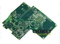
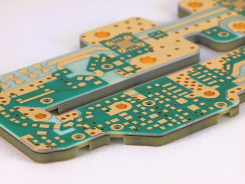
Base Material: FR4 Layer count: 4 layer Board thickness: 1.6mm Copper Thickness:1 oz Surface finish: nickel gold plating Soldermask Colors: Green Size:159.25*182/1up
At Barry: custom requests are common and welcome. We enjoy the challange. Extensive capabilities, wide material selection and state-of-the-art equiptment (including in-house plating and machining) ensure we can deliver a component fitting your exact
New Equipment | Fabrication Services
Low Cost Heavy Copper PCB China 4 Layers Circuit Boards Supplier Quick Details: FR4 base material 1.6mm board thickness 2oz heavy copper Plating gold finishing RF custom PCB boards Used for Radio Frequency From China PCB manufacturer Specifications
Double-Sided & Multi-Layer PCB Material: - FR-4 / Hi-Temp FR-4 / FR-5 / G10 / BT / Polyimide - Very Thin PCB: 0.004" 2L ~ 0.030" 8L - Thick Copper: 1/4 oz. ~ 11 oz. Process: - PTH - Blind/Buried/Segmented Via - Sequential Lamination - MicroVia Capa
New Equipment | Test Equipment
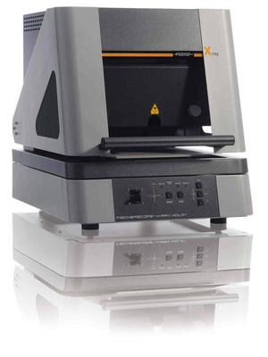
The Energy Dispersive X-Ray Fluorescence Analysis (ED-XRFA) is a method for measuring the thickness of coatings and for analyzing materials. It can be used for the qualitative and quantitative determination of the elemental composition of a material
New Equipment | Test Equipment
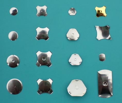
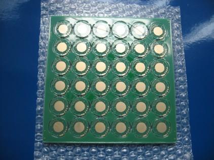
Metal dome (also named snap dome, tacticle domes) is the most improtant part of the switches. The metal domes are mainly use in the membrane switches, printed circuit boards, flexible circuit boards. The raw material is the thickness from 0.05mm to 0
1). 1+C+1 HDI, blind L1-L5/L5-L8 vias. 2). FR-4 Material, 1 oz weight. 3). 8 layer, 1.6mm thick. 4). 4/4 mils track and space 5). Min.drill 0.1mm 6). Green solder mask/ white silkscreen 7). Immersion gold over nickel
New Equipment | Assembly Services
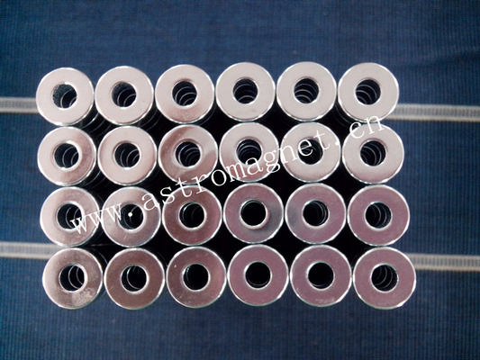
• Material: neodymium iron boron • Properties: high coercive force, the maximum working temperature is up to 200°C • Grades: N35 to N52, 33M to 48M, 33H to 48H, 30SH to 45SH, 30UH to 38UH and 30EH to 35EH • Shapes and size: disc, block, ring and s
General specification for Microwave/RF PCB Layer count: 1-6 Board thickness: 0.2-3.2mm Copper thickness: 0.5-4oz Dielectric Constant(DK): 2.2-10.3 Min trace width/spacing: 4/4mil Min drill hole size: 0.2mm Surface treatment: HAL(Lead free), I
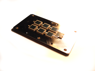
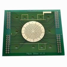
Consisting of multiple laminates and differing dielectric constants, this multilayer (displayed right) is a mixed-dielectric printed circuit board which was manufactured for the Aerospace Industry. Multilayer Mixed Dielectric PCB Specifications:


