Agile Circuit Co., Ltd is an experienced professional supplier of printed circuits. We are specialized in meeting your needs in all PCBs
Industry Directory | Manufacturer
Sprint Circuits,a high technology PCB manufacturing company,Since 2001.Our advantages are quick turn,Thick copper(up to 6oz) ,impendace control and high precision from 6layer to 12layer boards.
New Equipment | Rework & Repair Equipment
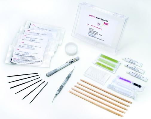
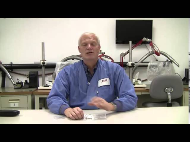
Poor handling procedures may sometimes damage corners and edges on printed circuit boards. Most of these types of damage to PCB's can be repaired using the BEST Board Repair Kit. This versatile repair kit along with our clear "how to" instructions of
New Equipment | Rework & Repair Equipment
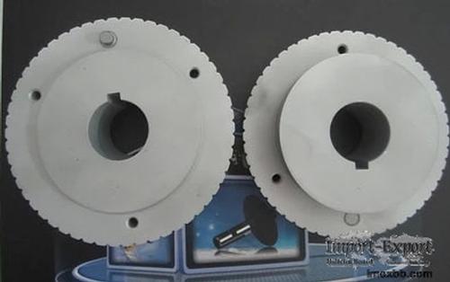
BEST circuit frames come in both dry film and epoxy versions. We can produce circuit frames in 1 and 2 oz copper as well as with shiny tin or nickle gold coating. These circuit frames are microetched on the board side in order to insure better adhesi
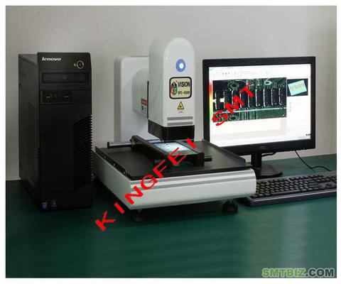
Used SMT Equipment | SPI / Solder Paste Inspection
Product Details of 3D SPI-6500 Thick Paste Measurement Instrument Product Functions 1, friendly programming interface 2, a variety of measurement methods 3, scan spacing adjustable 4, image 3D simulation function 5, independent 3D dynamic obser
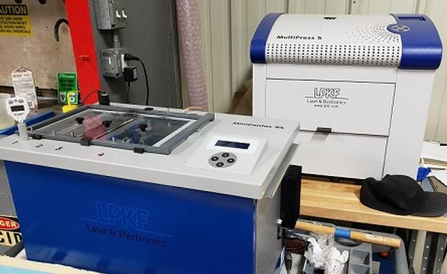
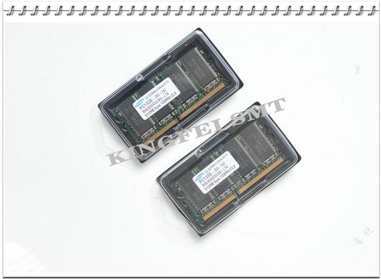
Used SMT Equipment | General Purpose Equipment
Package offers preferred: 1.) Protomat S103 Jetstream Dust Extraction System 4 Replacement Bags 3 new Vacuum table backers 1 used tight tolerance vacuum backer with sinter plate Solder Paste Dispensing attachment Upgraded to new Aluminum work
Industry News | 2009-10-17 09:43:47.0
Reduce PCB Repair Costs
Technical Library | 2020-07-22 19:39:05.0
The PWB industry needs to complete reliability testing in order to define the minimum copper wrap plating thickness requirement for confirming the reliability of PTH structures. Predicting reliability must ensure that the failure mechanism is demonstrated as a wear-out failure mode because a plating wrap failure is unpredictable. The purpose of this study was to quantify the effects of various copper wrap plating thicknesses through IST testing followed by micro sectioning to determine the failure mechanism and identify the minimum copper wrap thickness required for a reliable PWB. Minimum copper wrap plating thickness has become an even a bigger concern since designers started designing HDI products with buried vias, microvias and through filled vias all in one design. PWBs go through multiple plating cycles requiring planarization after each plating cycle to keep the surface copper to a manageable thickness for etching. The companies started a project to study the relationship between Copper wrap plating thickness and via reliability. The project had two phases. This paper will present findings from both Phase 1 and Phase 2.
Technical Library | 2023-11-14 19:52:11.0
The continuous drive in the Electronics industry to build new and innovative products has caused competitive design companies to develop assemblies with consolidated PCB designs, decreased physical sizes, and increased performance characteristics. As a result of these new designs, manufacturers of electronics are forced to contend with many challenges. One of the most significant challenges being the processing of thru-hole components on high thermal mass PCBs having the potential to exceed 20 layers in thicknesses and have copper mass contents of over 40oz. High thermal mass PCBs, coupled with the use of mixed technologies, decreased component spacing, and the change from Tin Lead Solder to Lead Free Alloys has lead many manufacturing facilities to purchase advanced soldering equipment to process challenging assemblies with a high degree of repeatability.

This video is on the repair of damaged corners presented by the professional instructing staff at BEST Inc. Corners get damaged from improper handling, storage or packaging. The repair of these damaged corners for multiple angles including both abov
Training Courses | | | IPC-6012 Trainer (CIT)
The Certified IPC-6012 Trainer (CIT) courses recognize individuals as qualified trainers in the area of design, fabrication and inspection of rigid printed boards and prepare them to deliver Certified IPC-6012 Specialist (CIS) training.
Training Courses | | | IPC-6012 Expert (CSE)
The IPC-6012 CSE program confirms that an individual has demonstrated the level of knowledge and understanding required to act as a subject matter expert for the IPC-6012 standard.
Events Calendar | Tue Jul 02 18:30:00 UTC 2024 - Tue Jul 02 18:30:00 UTC 2024 | ,
Europe Chapter Webinar: "Back-to-Basics" SMT Assembly
Career Center | Toronto,, Ontario Canada | Engineering,Research and Development
DEBTANU BASU 40 Fountain Head Road Toronto, ON M3J2V1 (416) 514 0619 Cell: 416 258 7488 E-mail: debtanubasu@aol.com With more than six years of experience in the field of flip chip technologies seeking a challenging technical position in the field
Career Center | Stoneham, | Engineering,Production,Research and Development,Technical Support
Warren P. Pumyea 8 Beacon Street Stoneham, Massachusetts 02180 Cell #: 978-821-7335 * E-mail: warren@pumyea.com http://www.pumyea.com/Process_Manufacturing_Engineer.doc Objective: Seeking a position as an engineer or related discipline whic
SMT Express, Issue No. 4 - from SMTnet.com Volume 1, Issue No. 4 Tuesday, September 14, 1999 Featured Article Return to Front Page MULTILAYER BOARD (MLB) CONSTRUCTIONS FOR HIGHEST LAMINATE INTEGRITY, DIMENSIONAL STABILITY, AND ELECTRICAL
Imagineering, Inc. | https://www.pcbnet.com/quote/board-quote-usa/?cpn=1
. PCB Specifications View Matrix Part Number * Revision Quantity * Thickness 0.062" Layers * Select One 2 4 Dimensions * Materials FR4(130Tg) FR4(180Tg) from Taiwan or China Copper Weight 1 oz 4 oz Cu from Taiwan or China Finish Plating Leaded Solder ENIG2U"-5U