
Wafer-level Product In-line(Ireland) 2D, 3D CT AXI Machine Automatic inspection equipment exclusively for the Wafer-level products and ultra-fine defects of mm can be detected using the Nano Tube of Class Focal spot 200nm. 2D, as well as 70&o
New Equipment | Test Equipment
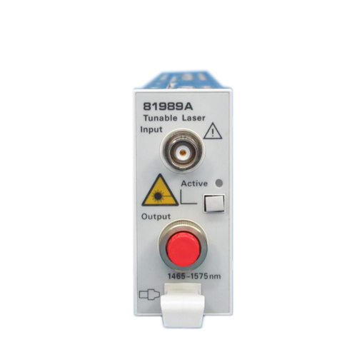
81989A Main features Wavelength range 1505 to 1630 nm Scanning wavelength accuracy ±10 pm Maximum scanning speed 200 nm/s Repetition rate of more than 2 times/sec for bidirectional scanning Built-in correlation control, stimulated Brillouin sca
Electronics Forum | Tue Oct 26 11:01:54 EDT 2004 | Simon UK
DO you have an xray onsite? One suggestion is to check what you can with that machine, i know it wont be able to magnify to 200nm or something, but it will show any ESD damage to the wire bonds or any major cracks of the silicon die. P.s. Most devi
Used SMT Equipment | X-Ray Inspection
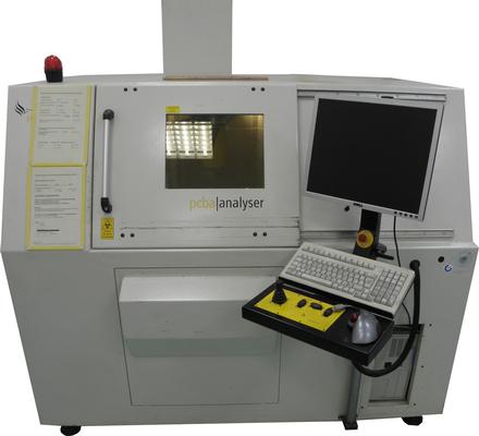
we herewith offer: Phoenix PCBA Analyser 160 NF Microfocus X-Ray system for the inspection of assembled boards, consisting of the X-Ray system, digital image acquisition and CNC. geometric magnification up to 2060 X total magnificatio
Industry News | 2011-05-27 21:57:47.0
Traqu is a high-resolution digital 3-D inspection device from Essemtec used for 3-D measurement and analysis in processes such as solder paste inspection (SPI). Measurement tasks are programmed with a few mouse clicks, and DXF and Gerber data can be imported.
Industry News | 2019-12-16 22:05:41.0
In recent years, as a subdivision of the LED industry, UV LED industry has developed in full swing. In 2019, the UV LED industry is in the buffer phase of application explosion, and the most urgent task for relevant companies is to launch the technology war, in order to capture as many places as possible before the real market explosion.
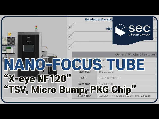
#Xray#Inspection#SEC Nano-focus Tube of 200 nano resolution which is specialized for sub-micron defects of Semiconductor Packaging, Wafer Level Packaging(WLP). -Non-destructive Analysis System -High-Resolution Image with Dual Type CTs -Application
| Sm | t | net |
| 1 |


