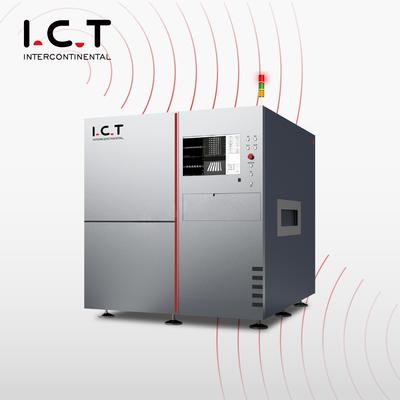
Inline 3D PCB Automated X-ray Inspection System - Advanced Quality Assurance Solution ❙ Introduce of SMT PCBA X-ray Machine Explore our Inline 3D PCB Automated X-ray Inspection System, a cutting-edge solution for advanced quality assurance in PCB
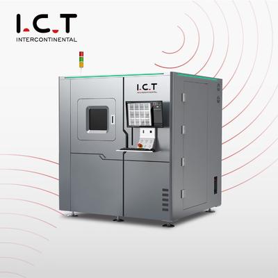
Off-line 3D SMT X-ray Inspection Machine - High-precision Quality Control ❙ Introduce of SMT PCBA X-ray Machine Looking for an off-line 3D SMT X-ray inspection machine? Our high-precision 3D SMT X-ray machine ensures top-notch quality control for
Industry News | 2026-02-16 15:29:38.0
The SMTA Capital Chapter is pleased to announce an upcoming technical webinar focused on an increasingly critical reliability risk in modern electronics manufacturing: component failure resulting from overexposure to ionizing radiation during manual X-ray solder joint inspection.
Industry News | 2018-04-11 20:04:01.0
SMTA Europe announces Session 3 Technical Program on Advanced Test Methods at the “Electronics in Harsh Environments Conference” to be held in Amsterdam, Netherlands, on April 25th, 2018.
Technical Library | 2024-11-22 06:29:45.0
This article discusses the critical importance of identifying faulty components in Printed Circuit Boards (PCBs). It outlines common signs of defective components--such as physical damage, electrical failures, and overheating--while also exploring detection techniques like visual inspection, multimeter testing, thermal imaging, and X-ray analysis. Emphasizing the significance of choosing a reliable PCB manufacturing partner, the article highlights how proactive detection can ensure greater reliability and longevity in electronic devices. For businesses seeking comprehensive PCB solutions, the article encourages engaging with specialized manufacturers to optimize their PCB projects and enhance product quality.
Inline 3D PCB Automated X-ray Inspection System - Advanced Quality Assurance Solution ❙ Introduce of SMT PCBA X-ray Machine Explore our Inline 3D PCB Automated X-ray Inspection System, a cutting-edge solution for advanced quality assurance in PCB
Off-line 3D SMT X-ray Inspection Machine - High-precision Quality Control ❙ Introduce of SMT PCBA X-ray Machine Looking for an off-line 3D SMT X-ray inspection machine? Our high-precision 3D SMT X-ray machine ensures top-notch quality control for
SMTnet Express, July 10, 2014, Subscribers: 22902, Members: Companies: 13928, Users: 36450 Fatigue Damage Behavior of a Surface-mount Electronic Package Under Different Cyclic Applied Loads. Ren Huai-Hui, Wang Xi-Shu - Wind Power Engineer
| http://www.thebranfordgroup.com/dnn3/Auction/BENC0423.aspx
. We provide the names and contact information of available companies solely as a courtesy to our buyers. The Branford Group does not endorse or guarantee the services of any machinery rigging, transport or export company, and cannot be held responsible for any damage, omission or other problems incurred
| https://www.smtfactory.com/pcb-x-ray-inspection-machine
I.C.T Solutions Rising to New Heights: Elevating the PCB X-ray Inspection machine with High-End I.C.T Solutions Views: 0 Author: I.C.T Publish Time: 2023-09-13 Origin: www.smtfactory.com Inquire In the world of advanced electronics manufacturing, the importance of PCB X-ray Inspection Machines cannot be overstated


