Industry Directory | Manufacturer
Test fixtures for fine pitch applications to 6 mils center to center spacing.
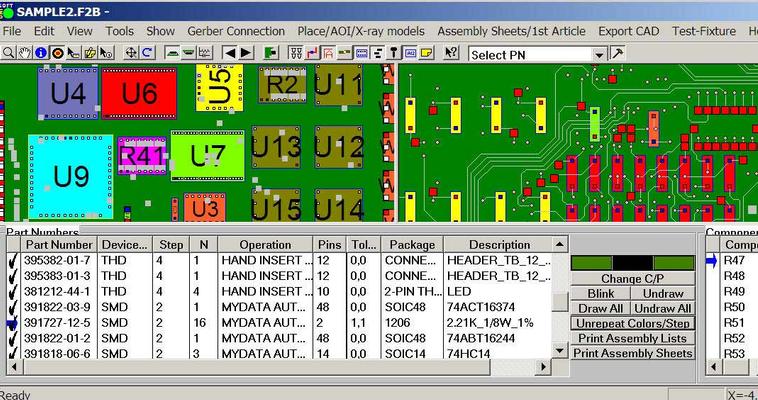
ProntoVIEW-MARKUP is assembly CAD Viewer & Gerber Viewer software used by electronics manufacturers to quickly find components, pin, shorts between traces, etc. ProntoVIEW-MARKUP is also a redline tool that allows annotation of the assembly to creat
New Equipment | Fabrication Services
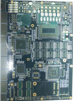
HDI PCB Manufacturer & Assembly – One-stop services from China -HDI (high-density interconnection board) is a compact circuit board designed for small capacity users. Compared with ordinary PCB, the most significant feature of HDI is that the wiri
Electronics Forum | Wed Sep 18 12:35:56 EDT 2002 | stepheno
Fourth - > back to design of PCB. Are there solder dams of > mask between the pads? If yes, that helps. If > not, pay close attention to stencil aperture > width and be sure that the aperture deposits less > paste by 1-2 mils per pad, centered o
Electronics Forum | Wed Sep 18 12:31:16 EDT 2002 | dragonslayr
My suggestion is to conduct a Design For Manufacturing (DFM)study on the assembly in question. Pay particular attention to the pad sizes, component lead dimensions and satisfy yourself that those two factors are correct. Given that pads match compone
.jpg)
Used SMT Equipment | Assembly Accessories
E BY DEK DEK’s experienced printing specialists have developed an innovative platform for E by DEK with high-quality components, sophisticated construction, and modular design that guarantees a stable and reliable printing process even for the latest
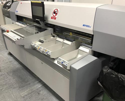
Used SMT Equipment | Pick and Place/Feeders
Make: Mycronic Model: My200SX-14 Vintage: 2014 Software Version: TPSys 3.1.1c for Ubuntu Linux Details: • Electrical Two-Pole Test • Electrical Transistor Test • Optica
Industry News | 2003-06-04 09:19:23.0
With increasing demand for fine pitch placements and a growing amount of fast turnaround high-tech low-volume prototype work, Speedboard has invested in additional SMT/BGA placement/rework equipment.
Technical Library | 2023-07-25 16:50:02.0
Some of the new handheld communication devices offer real challenges to the paste printing process. Normally, there are very small devices like 01005 chip components as well as 0.3 mm pitch uBGA along with other devices that require higher deposits of solder paste. Surface mount connectors or RF shields with coplanarity issues fall into this category. Aperture sizes for the small devices require a stencil thickness in the 50 to 75 um (2-3 mils) range for effective paste transfer whereas the RF shield and SMT connector would like at least 150 um (6 mils) paste height. Spacing is too small to use normal step stencils. This paper will explore a different type of step stencil for this application; a "Two-Print Stencil Process" step stencil. Here is a brief description of a "Two-Print Stencil Process". A 50 to 75 um (2-3 mils) stencil is used to print solder paste for the 01005, 0.3 mm pitch uBGA and other fine pitch components. While this paste is still wet a second in-line stencil printer is used to print all other components using a second thicker stencil. This second stencil has relief pockets on the contact side of the stencil any paste was printed with the first stencil. Design guidelines for minimum keep-out distances between the relief step, the fine pitch apertures, and the RF Shields apertures as well relief pocket height clearance of the paste printed by the first print stencil will be provided.
Technical Library | 1999-05-07 08:45:39.0
Fine pitch SMT devices, although certainly not new, present more of an assembly processing challenge than 50 mil pitch devices. In fact it seems that the finer the pitch the more difficult or narrower the process window becomes. Besides the pitch of the leads being less on fine pitch devices narrower pad width on the board is typical. With fine pitch designs the board fabrication process is also stressed in that the strip of mask between the pads is designed narrower, the alignment of the mask to copper becomes more critical

ITW EAE, the Electronic Assembly Equipment division of ITW is introducing an innovative new twin-nozzle developed by the Vitronics Soltec team for the ZEVA Selective Soldering System. The 3D-Twin-Nozzle™ has two nozzle diameters combined in one
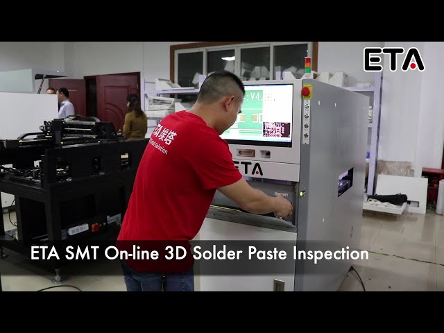
SMT On-line 3D Solder Paste Inspection If you could not find any similar items you want, you may send some photos to us. because our catalog and website haven't included all of our products. solder paste inspection,SMT SPI,SPI machine, SPI in
Training Courses | | | IPC-7711/7721 Specialist (CIS) Recert.
The Certified IPC-7711/7721 Specialist (CIS) recertification courses are intended for those individuals who were previously certified as IPC-7711/7721 Specialist.
Training Courses | | | IPC-7711/7721 Trainer (CIT)
The Certified IPC-7711/7721 Trainer (CIT) courses recognize individuals as qualified trainers in the area of rework and repair of printed boards and electronic assemblies and prepares them to deliver Certified IPC-7711/7721 (CIS) training.
Events Calendar | Wed May 31 00:00:00 EDT 2023 - Wed May 31 00:00:00 EDT 2023 | Holtsville, New York USA
Long Island Chapter Meeting: Fine Feature Paste Printing, Stencil Design and Solder Technology
Events Calendar | Mon Mar 18 00:00:00 EDT 2019 - Mon Mar 18 00:00:00 EDT 2019 | ,
Webinar: Stencil Design for Solder Paste, In Process Inspection & Process Defects
Career Center | Bangalore, India | Engineering,Maintenance,Production,Technical Support
SMT Stencil designing & Knowledge of full SMT process software known CAD/CAM -circuit CAM Pro 7.3,GC Power station, GCCAM Edit,Auto CAD, Fault finding of Electronic Boards & Servicing electronic machines.
Career Center | Bangalore-560026, Karnataka India | Engineering,Maintenance,Technical Support
New Product Introduction & Product dovelopment
SMTnet Express, December 31, 2015, Subscribers: 23,946, Members: Companies: 14,865, Users: 39,660 Study on Solder Joint Reliability of Fine Pitch CSP Yong Hill Liang, Hank Mao, YongGang Yan, Jindong (King) Lee; AEG, Flex (Flextronics International
PCB Libraries, Inc. | https://www.pcblibraries.com/Forum/pad-to-pad-space-in-3pin-sofl_topic2836.html
. You can't have a pin pitch of 0.175 when the maximum lead thickness is 0.23. That's impossible. Turn the minimum pad to pad off for micro-miniature packages. The pin pitch is 0.175. This can't be true


.gif)
winsouce.jpg)