Industry Directory | Manufacturer
UWELLPCB.com is the PCB supplier. We offer PCB from single side board, double side PCB to 32layer board,including the Rigid PCB, Flex PCB, Rigid-flex PCB,Quick-turn prototype and PCB assembly
New Equipment | Education/Training
This two day course is based on the IPC-7721. Students will learn how to repair surface mount pads, BGA pads, finger contacts, traces, laminate, plated through holes and more. Students will be introduced to the proper techniques for SMT & PTH compon

The PCB Footprint Expert is a powerful CAD library development tool powered by our own proprietary CAD LEAP Technology (Libraries Enhanced with Automated Preferences). It is packed with very powerful advanced library management features that cuts foo
Electronics Forum | Fri Jan 21 13:27:38 EST 2011 | mosborne1
Try baking your boards first to remove the moisture. Moisture and boards that have not been drilled properly will cause pin hole or blow holes in PTH. Also take a look the surface of the pads before printing. You maybe contaminating the surfaces of t
Electronics Forum | Thu Jan 20 11:02:46 EST 2011 | dyoungquist
Armando Link does not work. Goes to a "page not found" error in flickr.
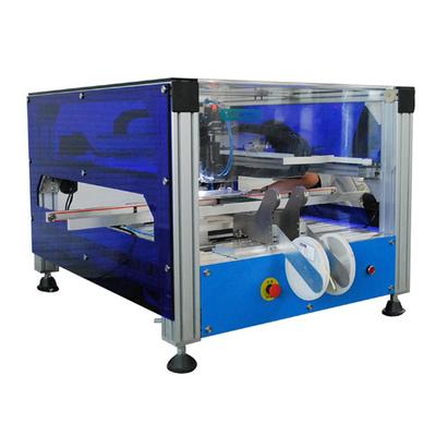
Used SMT Equipment | Pick and Place/Feeders
Automatic pick and place machine TP400V is the high cost-effective equipment in the market, it can pick and place variety of components by its vacuum nozzle. The machine can mount 0603、 SOIC、PLCC、QFP IC and many SMD chip components; optional vision

Used SMT Equipment | Pick and Place/Feeders
Automatic pick and place machine 210 is the high cost-effective equipment in the market, it can pick and place variety of components by its vacuum nozzle. The machine can mount 0402、 SOIC、PLCC、QFP IC and many SMD chip components; optional vision pos
Industry News | 2018-10-18 11:19:07.0
How To Design Cost-Effective PCBs
.png)
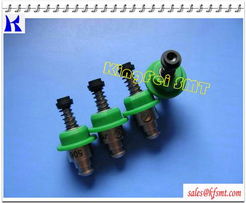
Parts & Supplies | Assembly Accessories
YAMAHA KV8-M7710-A0X 71A YAMAHA KV8-7760-00X Nozzle 76A 5322 360 10496 YAMAHA KV8-M7730-00X Nozzle 73A YAMAHA KV8-M7720-A1X Nozzle 72A YAMAHA LC2-M7720-A0X Nozzle 82A K
Parts & Supplies | SMT Equipment
500/501/502/503/504/505/506/507/508 series nozzle for SMT JUKI machine KE2010——2040 PART No. PART NAME SIZE(mm) REMARKS E3608-729-0A0 #500 ASS'Y(2-HOLES) 0.5/1.0 E3600-729-0A0 #501 ASS'Y φ0.7/φ0.2 E3601-729-0A0 #502 ASS'Y φ0.7/φ0.4 E3602-729-0
Technical Library | 2023-06-12 18:52:18.0
This paper will review stencil design requirements for printing solder paste around and in through-hole pads / openings. There is much interest in this procedure since full implementation allows the placement of both through-hole components as well as SMD's and the subsequent reflow of both simultaneously. This in turn eliminates the need to wave solder or hand solder through-hole components.
Technical Library | 2019-10-10 00:26:28.0
Voids are a plague to our electronics and must be eliminated! Over the last few years we have studied voiding in solder joints and published three technical papers on methods to "Fill the Void." This paper is part four of this series. The focus of this work is to mitigate voids for via in pad circuit board designs. Via holes in Quad Flat No-Lead (QFN) thermal pads create voiding issues. Gasses can come out of via holes and rise into the solder joint creating voids. Solder can also flow down into the via holes creating gaps in the solder joint. One method of preventing this is via plugging. Via holes can be plugged, capped, or left open. These via plugging options were compared and contrasted to each other with respect to voiding. Another method of minimizing voiding is through solder paste stencil design. Solder paste can be printed around the via holes with gas escape routes. This prevents gasses from via holes from being trapped in the solder joint. Several stencil designs were tested and voiding performance compared and contrasted. In many cases voiding will be reduced only if a combination of mitigation strategies are used. Recommendations for combinations of via hole plugging and stencil design are given. The aim of this paper is to help the reader to "Fill the Void."

The PCB Footprint Expert is a powerful CAD library development tool powered by our own proprietary CAD LEAP Technology (Libraries Enhanced with Automated Preferences). It is packed with very powerful advanced library management features that cuts foo

This video is on the dry film pad repair technique per IPC 7721 standards. BEST professional instructors demonstrate the proper technique for the repair for PCB pads using the dry film. http://www.solder.net More on PCB pad repair here: http://www.s
Training Courses | | | IPC-7711/7721 Specialist (CIS) Recert.
The Certified IPC-7711/7721 Specialist (CIS) recertification courses are intended for those individuals who were previously certified as IPC-7711/7721 Specialist.
Training Courses | | | IPC-7711/7721 Trainer (CIT)
The Certified IPC-7711/7721 Trainer (CIT) courses recognize individuals as qualified trainers in the area of rework and repair of printed boards and electronic assemblies and prepares them to deliver Certified IPC-7711/7721 (CIS) training.
Events Calendar | Wed Dec 06 00:00:00 EST 2017 - Wed Dec 13 00:00:00 EST 2017 | Rolling Meadows, Illinois USA
X-Ray of PCBs Webtorial
Events Calendar | Tue Jan 23 00:00:00 EST 2018 - Tue Jan 23 00:00:00 EST 2018 | New Milford, Connecticut USA
FREE Webinar: Eliminate Circuit Board Problems and Failure Modes
Career Center | Bangalore, India | Engineering,Maintenance,Production,Technical Support
SMT Stencil designing & Knowledge of full SMT process software known CAD/CAM -circuit CAM Pro 7.3,GC Power station, GCCAM Edit,Auto CAD, Fault finding of Electronic Boards & Servicing electronic machines.
SMT Express, Volume 2, Issue No. 3 - from SMTnet.com Volume 2, Issue No. 3 Thursday, March 16, 2000 Featured Article Return to Front Page Stencil Design for Mixed Technology Through-hole / SMT Placement and Reflow by William E. Coleman, Photo
ORION Industries | http://orionindustries.com/pdfs/SILPAD900S.pdf
Gap Pad? 1500 Sil-Pad® 900S High Performance Insulator for Low Pressure Applications The Bergquist Company The Bergquist Company-Europe The Bergquist Company-Asia North American Headquarterss Bramenberg 9a 9F-1, No
Imagineering, Inc. | https://www.pcbnet.com/capabilities/fabrication/tolerances/
″ over finished hole size for vias and + 0.012″ over finished hole size for component holes. This means the annular ring (radius of the pad) should be at least


