Industry Directory | Manufacturer
Porous ceramic vacuum chuck table or Polishing Chuck table supplied to semiconductor industry for silicon wafer dicing or finishing purposes. This product is an uniform compact frame, high strength, g
Welcome to the next generation in PWB test solutions. We combine an exceptional team of technology and applications experts with HIOKI's industry-leading systems to enhance your reliability and to speed up your product development process.
New Equipment | Rework & Repair Services
PCB Repair Services BEST is your experienced resource for high value added PCB repair services. If you need any of the following completed to your printed circuit board then let the experts at BEST be your answer: Pad repair services Pad replace

New Equipment | Rework & Repair Equipment
The BEST PCB Epoxy Repair Kit can be used to repair lifted pads and traces as well as build up and repair edge corner damage to PCBs or repair solder mask which has been damaged or removed. By adding colorants a pcb color epoxy kit can be made up cus
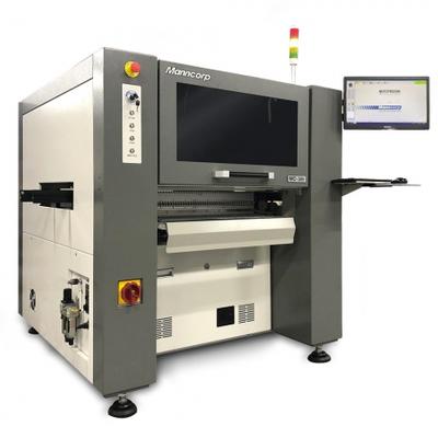
Used SMT Equipment | Pick and Place/Feeders
Heavy-duty, welded steel base frame w/ adjustable foot pads High-precision ball screw X-Y drive mechanism w/ linear encoders Three pick and place heads, each with servo-driven Z- and ?-axis motors Standard on-the-fly vision alignment cameras for c
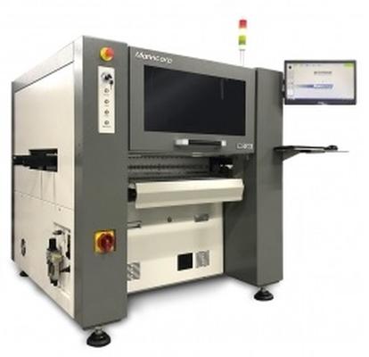
Used SMT Equipment | Pick and Place/Feeders
MC389CY-F3-V MC-389 High-Speed, High-Mix Pick & Place WITH CONVEYOR Heavy-duty, welded steel base frame w/ adjustable foot pads High-precision ball screw X-Y drive mechanism w/ linear encoders Three pick and place heads, each with servo-drive
Industry News | 2003-02-07 08:34:04.0
Featuring Individual Instructors who, for Approximately 90 Minutes Each, will Speak on a Timely and Specific Topic
Industry News | 2015-07-06 10:34:12.0
The SMTA announces a new feature area that will debut during the SMTA International Electronics Exhibition: the “SMTA - NPL Solder Paste and Solder Joint Automatic Inspection Experience.” This special feature will take place during both days of the SMTA International Exhibition at the Donald Stephens Convention Center in Rosemont, Illinois on September 29 - 30, 2015.
.jpg)
Technical Library | 2023-05-02 19:03:34.0
The demand for 0201 components in consumer products will increase sharply over the next few years due to the need for miniaturization. It is predicted that over 20 billion 0201 components will be used in more than one billion cell phones worldwide by the year 2003. Therefore, research and development on 0201 assembly is becoming a very hot topic. The first step to achieve a successful assembly process is to obtain a good PCB design for 0201 packages. This paper presents the data and criteria of PCB design for 0201 packages, including the pad design for 0201 components, and the minimum pad spacing or component clearance between 0201 components or between 0201 and other components. A systematic study on pad design and pad spacing was undertaken, using two test vehicles and three Design of Experiments (DOEs). In the first DOE, 2 out of 18 types of 0201 pad designs were selected based on process yield. The second DOE was focused on pad spacing, including 10mil, 8mil, 6mil and 4mil. The third experiment was final optimization, using two types of optimized pad designs with 10mil, 8mil and 6mil pad spacing. Through the above experiments, the design guideline for PCB layout for 0201 packages and the assembly process capability are identified.
Technical Library | 2017-09-07 13:56:11.0
As a surface finish for PCBs, Electroless Nickel/Electroless Palladium/Immersion Gold (ENEPIG) was selected over Electroless Nickel/Immersion Gold (ENIG) for CMOS image sensor applications with both surface mount technology (SMT) and gold ball bonding processes in mind based on the research available on-line. Challenges in the wire bonding process on ENEPIG with regards to bondability and other plating related issues are summarized.

PCB pad repair technique demonstrated using the 2-part epoxy method. More on this PCB pad repair technique: http://www.solder.net/services/pcb-repair/pad-and-trace-repair/ More on the recommended epoxy: http://www.soldertools.net/pcb-repair-epoxy-r
03059051-01 Lifting Table Dual Conveyor X4i 03059195-01 Retrofit kit pneumatic unit D1 03059196-01 Gas Spring 400N ( for D1/D2 Left Hood) 03059238S01 Linear Dipping Unit (LDU) Basis 03059375-01 Starter kit filter disc 2-parts / C+
Training Courses | | | IPC-7711/7721 Trainer (CIT)
The Certified IPC-7711/7721 Trainer (CIT) courses recognize individuals as qualified trainers in the area of rework and repair of printed boards and electronic assemblies and prepares them to deliver Certified IPC-7711/7721 (CIS) training.
Training Courses | | | IPC-7711/7721 Specialist (CIS)
The Certified IPC-7711/7721 Specialist (CIS) training focuses on rework of electronic assemblies and repair and modification of printed boards and electronic assemblies.
Events Calendar | Sun Apr 11 18:30:00 UTC 2021 - Sun Apr 11 18:30:00 UTC 2021 | ,
Europe Chapter Webinar: Tombstoning Components during Reflow Soldering - Causes & Cures
Events Calendar | Tue May 30 18:30:00 UTC 2023 - Tue May 30 18:30:00 UTC 2023 | Holtsville, New York USA
Long Island Chapter Meeting: Fine Feature Paste Printing, Stencil Design and Solder Technology
SMTnet Express, May 4, 2023, Subscribers: 24,706, Companies: 11,774, Users: 27,931 █ Electronics Manufacturing Technical Articles Stencil Printing 008004/0201 Aperture Components This paper will focus on the application requirements
| http://etasmt.com/cc?ID=te_news_industry,24564&url=_print
. According to the IPC standard, non-wetting is defined as the inability of molten solder to form a metallic bond with the base metal. This results in the PCB pads or the
| https://www.eptac.com/blog/5-common-solder-mistakes-and-how-to-resolve-them
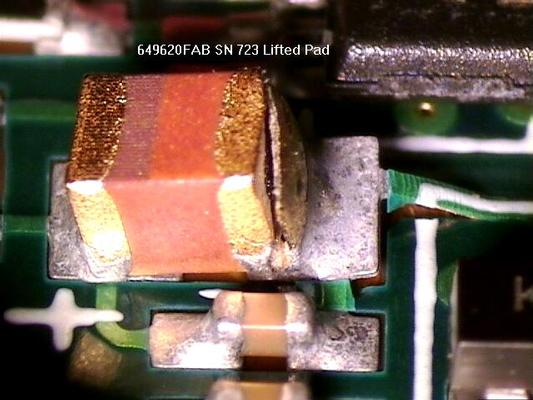
. Lifted pads result in improper connections, and while they can be repaired, it’s not always easy. The most practical way is to fold the solder lead over and bond it to a copper trace that’s still intact. If


