Industry Directory | Research Institute / Laboratory / School
The Technological Educational Institute of Athens was a state higher educational institute in Athens, only for applied sciences. Founded in 1983, it originated from one of the first five Centres for Higher Technical Education ...
Industry Directory | Research Institute / Laboratory / School
BME is considered the world's oldest Institute of Technology which has university rank and structure. It was the first institute in Europe to train engineers at university level.

The PCB Footprint Expert is a powerful CAD library development tool powered by our own proprietary CAD LEAP Technology (Libraries Enhanced with Automated Preferences). It is packed with very powerful advanced library management features that cuts foo
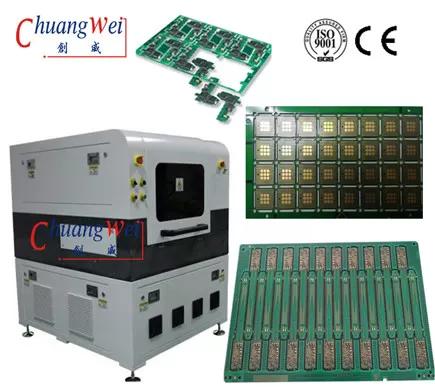
Features: 1 High Accuracy: The combination of a low-drift galvanometer and a fast ironless linear motor system platform enables fast cutting while maintaining micrometer-level accuracy; 2 easy to learn: independent research and development of Win
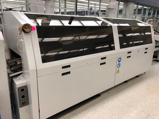
Used SMT Equipment | Soldering - Reflow
Vitronics 6622CC (Pb Free) Wave Soldering Machine Brand: Vitronics Model: 6622CC Vintage: 2001 Serial Number: 0103652201 LEADFREE unit Configured with Main Wave and Chip Wave Basic system according to General Specification (GS 235) CONTRO
Industry News | 2003-03-07 08:28:53.0
NPL now offers an on-site Lead-Free Health Check, where the issues brought to bear by lead-free are examined in the context of your company.
Industry News | 2003-06-05 08:11:23.0
Kerry co-solvent system pays for itself in 13 months
Technical Library | 2017-12-11 22:31:06.0
Typical printed circuit board assemblies (PCBAs) processed by reflow, wave, or selective wave soldering were analysed for typical levels of process related residues, resulting from a specific or combination of soldering process. Typical solder flux residue distribution pattern, composition, and concentration are profiled and reported. Presence of localized flux residues were visualized using a commercial Residue RAT gel test and chemical structure was identified by FT-IR, while the concentration was measured using ion chromatography, and the electrical properties of the extracts were determined by measuring the leak current using a twin platinum electrode setup. Localized extraction of residue was carried out using a commercial C3 extraction system. Results clearly show that the amount and distribution of flux residues are a function of the soldering process, and the level can be reduced by an appropriate cleaning. Selective soldering process generates significantly higher levels of residues compared to the wave and reflow process. For conformal coated PCBAs, the contamination levels generated from the tested wave and selective soldering process are found to be enough to generate blisters under exposure to high humidity levels.
Technical Library | 2018-09-21 10:12:53.0
Moisture accumulates during storage and industry practice recommends specific levels of baking to avoid delamination. This paper will discuss the use of capacitance measurements to follow the absorption and desorption behaviour of moisture. The PCB design used in this work, focused on the issue of baking out moisture trapped between copper planes. The PCB was designed with different densities of plated through holes and drilled holes in external copper planes, with capacitance sensors located on the inner layers. For trapped volumes between copper planes, the distance between holes proved to be critical in affecting the desorption rate. For fully saturated PCBs, the desorption time at elevated temperatures was observed to be in the order of hundreds of hours. Finite difference diffusion modelling was carried out for moisture desorption behaviour for plated through holes and drilled holes in copper planes. A meshed copper plane was also modelled evaluating its effectiveness for assisting moisture removal and decreasing bake times. Results also showed, that in certain circumstances, regions of the PCB under copper planes initially increase in moisture during baking.

The PCB Footprint Expert is a powerful CAD library development tool powered by our own proprietary CAD LEAP Technology (Libraries Enhanced with Automated Preferences). It is packed with very powerful advanced library management features that cuts foo
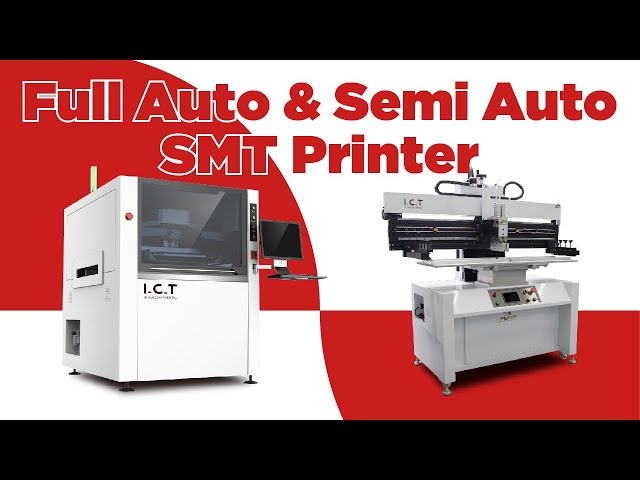
Full-auto SMT Stencil Printer is indispensable equipment in SMT production Line. It is generally composed of board mounting, solder paste, imprinting, and circuit board transfer. Widely used are Full-auto SMT Stencil Printer and semi-auto SMT Stencil
Events Calendar | Sun Feb 18 18:30:00 UTC 2024 - Sun Feb 18 18:30:00 UTC 2024 | ,
SMTA Webinar: Development of Wireless Strain Measurement for Printed Circuit Board
Events Calendar | Sun Jun 07 18:30:00 UTC 2020 - Sun Jun 07 18:30:00 UTC 2020 | ,
Practical Set-Up, Qualification of Cleaning Process in PCB Assembly
Career Center | Orange County, California USA | Quality Control
Job Description: Summary: Reporting to the COO/CTO the VP of Quality role will involve creating and/or augmenting the Quality system and programs to be a pro-active vs. a reactive structure. This will involve creating an overall quality vision, se
Career Center | Chandler, Arizona USA | Technical Support
Koh Young America is looking for technical field application engineers to support our world class electronics 3D measurement and inspection products. This a dynamic position and will require skills to handle both technical pre-sales activities, s
Career Center | Toronto,, Ontario Canada | Engineering,Research and Development
DEBTANU BASU 40 Fountain Head Road Toronto, ON M3J2V1 (416) 514 0619 Cell: 416 258 7488 E-mail: debtanubasu@aol.com With more than six years of experience in the field of flip chip technologies seeking a challenging technical position in the field
Career Center | Darien, Illinois USA | Engineering,Management,Production,Quality Control,Sales/Marketing
I have a wealth of experience in all phases of manufacturing industrial, electromechanical, and electronic products using a variety of processes such as metal working, machining, plastics extrusion, injection molding, and all forms of electronic and
Surface Mount Technology Association (SMTA) | https://www.smta.org/board_of_directors/criteria.cfm
Board of Directors Service Criteria 中文 MEMBERS LOGIN Membership Become a Member! Renew Membership About SMTA Ambassadors Benefits Classifications Member Directory Member Directory Corporate Suppliers Corporate Users Consultants List Advertisers Update Your Info
ASYMTEK Products | Nordson Electronics Solutions | https://www.nordson.com/en/divisions/march/about-us/events/wafer-level-packaging-symposium-2022
. One of these advanced technologies is silicon-based wafer-level packaging, such as fan-out wafer-level packaging. As the semiconductor industry shifts focus to more than