
Industry Directory | Training Provider / Manufacturer's Representative / Equipment Dealer / Broker / Auctions / Consultant / Service Provider
Products, services, training & consulting for the assembly, rework & repair of electronic assemblies. BGA process experts. Manufacturers Rep, Distributor & Service Provider for Seamark/Zhuomao and Shuttle Star BGA Rework Stations.
Industry Directory | Manufacturer
Dynamic Manufacturing specializes in Electronic Manufacturing Services: Surface Mount Printed Circuit Boards (PCB's), Through-hole PCB's, Prototyping, Testing, Inspection, Conformal Coating, Enclosures. Contract Design: Printed Circuit Boards, Temper
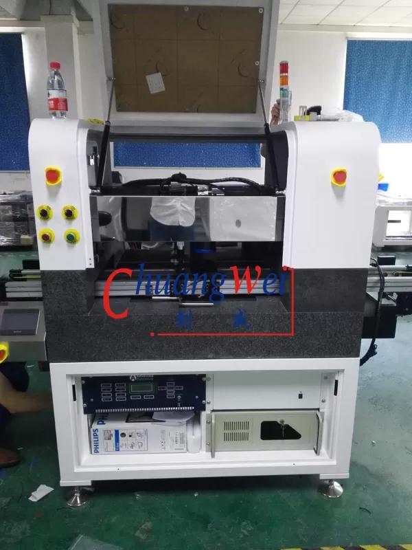
Features: 1 High Accuracy: The combination of a low-drift galvanometer and a fast ironless linear motor system platform enables fast cutting while maintaining micrometer-level accuracy; 2 easy to learn: independent research and development of Win
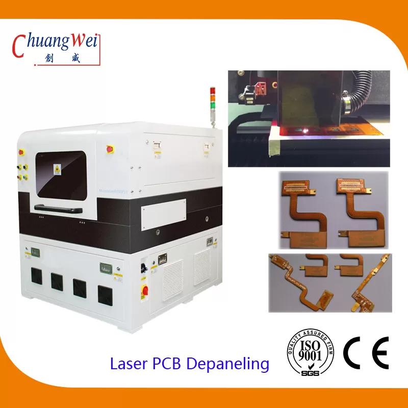
Features: 1. High precision CCD automatic positioning, automatic focusing. Fast and accurate positioning, save time and no worries; 2. Friendly interface,Simple operation, easy to use, free application; Small size, Save more space; rigorous secur
Electronics Forum | Wed Sep 15 23:15:55 EDT 2004 | pdeuel
Im with Pete, Zero defects. We have high defect rate for many reasons. No line tech, operators set up and run then when QA reports defects engneers are called. Not to make people mad but our process engneers are lacking practical experance to fix pro
Electronics Forum | Sun Apr 05 09:46:47 EDT 1998 | Earl Moon
| We are looking at reflow soldering some Flexi-rigid | pcbs. I have heard that IR reflow soldering can make the Polyimide "self heat" and cause de-lamination. | Does anyone have any info. The thermal problems associated with polyimide rigid/flex de
Used SMT Equipment | Soldering - Selective
Configuration: Universally Adjustable Tooling Carrier Inerted Nitrogen System Lead Free Capability (Titanium solder pot and pump assembly) Solder Wire Feeder with Solder bath level sensor Drop Jet Fluxer Programming Camera
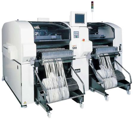
Used SMT Equipment | Chipshooters / Chip Mounters
Features: Fast Changeover for high mix environment. Re-configurable to A, B, or C types (A type – 8X8 heads, B type – 3X3 heads, C type – 8X3 heads) Flexible Heads- Large part ranges High Speed head- 0402(01005) – 24mm2 Multi Fu
Industry News | 2003-02-27 08:22:44.0
Circatex is to open its first satellite office in mainland Europe in France.
Technical Library | 2018-09-21 10:12:53.0
Moisture accumulates during storage and industry practice recommends specific levels of baking to avoid delamination. This paper will discuss the use of capacitance measurements to follow the absorption and desorption behaviour of moisture. The PCB design used in this work, focused on the issue of baking out moisture trapped between copper planes. The PCB was designed with different densities of plated through holes and drilled holes in external copper planes, with capacitance sensors located on the inner layers. For trapped volumes between copper planes, the distance between holes proved to be critical in affecting the desorption rate. For fully saturated PCBs, the desorption time at elevated temperatures was observed to be in the order of hundreds of hours. Finite difference diffusion modelling was carried out for moisture desorption behaviour for plated through holes and drilled holes in copper planes. A meshed copper plane was also modelled evaluating its effectiveness for assisting moisture removal and decreasing bake times. Results also showed, that in certain circumstances, regions of the PCB under copper planes initially increase in moisture during baking.
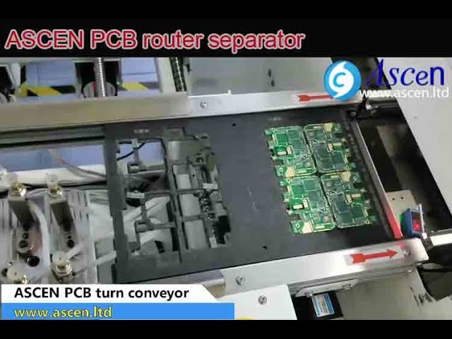
https://www.ascen.ltd PCB rotation conveyor PCB turn conveyor|180 degree or 90 degree turning rotational transport change PCB side direction output reflow oven for processing.auto PCB turn conveyor and PCB diverter changing the PCB conveying direct
PCB 90°turning conveyor and PCB turn diverter/PCB conveyor machine link: https://www.ascen.ltd/Products/Automatic_SMT_equipment/PCB_conveyor/95.html PCB 90°Turn conveyor is designed for changing the conveying direction of flow of a PCB production li
Training Courses | | | PCB Rework and Hand Soldering Courses
The PCB rework and hand soldering courses courses cover techniques of rework and repair of PCBs, BGAs and other electronics assemblies, and teach fundamentals of soldering of electronics assemblies.
Training Courses | | | Other Courses
Other courses related to electronics manufacturing and assembly
Events Calendar | Wed Apr 21 00:00:00 EDT 2021 - Wed Apr 21 00:00:00 EDT 2021 | ,
Oregon Chapter Tutorial: How Clean is Clean and How Do You Know for Sure?
Career Center | Kingston, Ontario, Ontario Canada | Sales/Marketing
We are a PCB manufacturer located in China and right now we have set up our office in Ontario, Canada. We can produce high-quality PCBs up to 24 layers and we accept orders for prototypes as well as large volumes, both with very competitive prices. W
Career Center | Columbus, Ohio USA | Engineering
LSI ADL Technology LLC., a fast growing Electronics Manufacturing Service Provider in Columbus, Ohio is currently seeking a Manufacturing Process Engineer for SM and TH PCB manufacturing processes. This position is hands on and requires flexibility o
Career Center | Bangalore, India | Engineering,Management,Production,Quality Control,Technical Support
WORK EXPERIENCE DETAILS: 7+ Years of Experience in manufacturing & hardware testing of Protocol conveter & Commissioning, Products delivery and QA/QC. 2+ Years of Experience in Hardware testing and Package Level testing. 2+ Years of Experience in
Career Center | BANGALORE, Karnataka India | Quality Control
New Model Evaluation • Testing & Evaluation of New TV models as per the relavant standards & release the defect free product for Mass Production • Measurement of audio parameters like Max out put, distotion, S/N ratio, hum, buzz etc • To conduct aud
PCB Libraries, Inc. | https://www.pcblibraries.com/Forum/RSS_ipc7351-or-manufacturer-recommended-footprint_topic2639.xml
PCB Libraries Forum : IPC-7351 or Manufacturer Recommended Footprint? PCB Libraries Forum : IPC-7351 or Manufacturer Recommended Footprint
Imagineering, Inc. | https://www.pcbnet.com/blog/what-are-lamination-voids-in-pcb-manufacturing/
Close Search What Are Lamination Voids in PCB Manufacturing? By Behind the Work June 16, 2022 September 21st, 2023 Blog , Industry News No Comments Lamination voids, also known as delamination, are a problem that can occur in the printed circuit board manufacturing process
Products, services, training & consulting for the assembly, rework & repair of electronic assemblies. BGA process experts. Manufacturers Rep, Distributor & Service Provider for Seamark/Zhuomao and Shuttle Star BGA Rework Stations.
Training Provider / Manufacturer's Representative / Equipment Dealer / Broker / Auctions / Consultant / Service Provider
1750 Mitchell Ave.
Oroville, CA USA
Phone: (888) 406-2830


