Industry Directory | Manufacturer
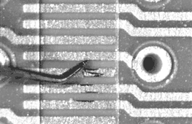
Test fixtures for fine pitch applications to 6 mils center to center spacing.
Industry Directory | Consultant / Service Provider
Specialised in Prototyping Assembly/Rework
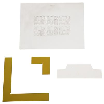
New Equipment | Solder Paste Stencils
SMT Foil Stencils are laser cut solder paste stencils designed to work on their own for hand printing or with stencil tensioning systems. These laser cut stencils do not need to be permanently glued in a frame. These so-called frameless stencils are
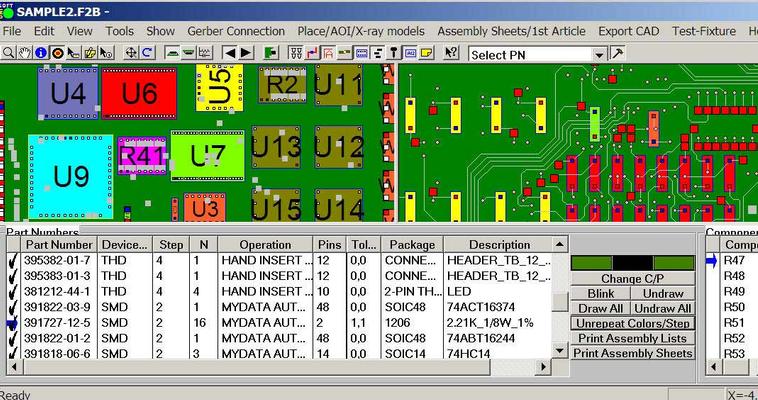
ProntoVIEW-MARKUP is assembly CAD Viewer & Gerber Viewer software used by electronics manufacturers to quickly find components, pin, shorts between traces, etc. ProntoVIEW-MARKUP is also a redline tool that allows annotation of the assembly to creat
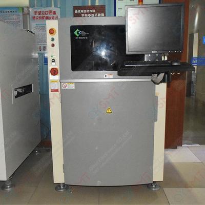
Used SMT Equipment | SPI / Solder Paste Inspection
Solder paste thickness detector Measurement software: MC-110-2.5D video observation, image storage, thickness measurement, data recording, background light, laser brightness control, area (square Shape, irregular polygon, circle) / volume / spacin
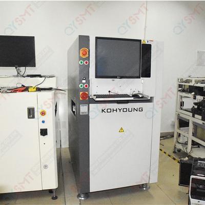
Used SMT Equipment | SPI / Solder Paste Inspection
KOH YONG/SPI KY8030 2XL MACHINE KY8030-2XL MC-110-2.5D video observation, image storage, thickness measurement, data recording, background light, laser brightness control, area (square, irregular polygon, circle)/volume/spacing (X, Y axis)/angle
Industry News | 2016-02-27 20:41:52.0
BEST Inc. instructors will be conducting 2 training sessions this year at the APEX Expo 2016 - Advanced Rework: Hands-on BGA Reballing, Lead-Free Devices, and Fine-Pitch Parts, and the 2nd session - Stencil Printing: Consistent Print Volumes for SMT Rework.
Industry News | 2018-12-08 03:29:29.0
SMT Dictionary – Surface Mount Technology Acronym and Abbreviation
Technical Library | 2023-01-17 17:58:36.0
Heterogeneous integration has become an important performance enabler as high-performance computing (HPC) demands continue to rise. The focus to enable heterogeneous integration scaling is to push interconnect density limit with increased bandwidth and improved power efficiency. Many different advanced packaging architectures have been deployed to increase I/O wire / area density for higher data bandwidth requirements, and to enable more effective die disaggregation. Embedded Multi-die Interconnect Bridge (EMIB) technology is an advanced, cost-effective approach to in-package high density interconnect of heterogeneous chips, providing high density I/O, and controlled electrical interconnect paths between multiple dice in a package. In emerging architectures, it is required to scale down the EMIB die bump pitch in order to further increase the die-to-die (D2D) communication bandwidth. Aa a result, bump pitch scaling poses significant challenges in the plated solder bump reflow process, e.g., bump height / coplanarity control, solder wicking control, and bump void control. It's crucial to ensure a high-quality solder bump reflow process to meet the final product reliability requirements. In this paper, a combined formic acid based fluxless and vacuum assisted reflow process is developed for fine pitch plated solder bumping application. A high-volume production (HVM) ready tool has been developed for this process.
Technical Library | 2013-07-03 10:31:54.0
It has been demonstrated in numerous pieces of work that stencil printing, one of the most complex PCB assembly processes, is one of the largest contributors to defects (Revelino et el). This complexity extends to prototype builds where a small number of boards need to be assembled quickly and reliably. Stencil printing is becoming increasingly challenging as packages shrink in size, increase in lead count and require closer lead spacing (finer pitch). Prototype SMT assembly can be further divided between industrial and commercial work and the DIYer, hobbyist or researcher groups. This second group is highly price sensitive when it comes to the materials used for the board assembly as their funds are sourced from personal or research monies as opposed to company funds. This has led to development of a lower cost SMT printing stencil made from plastic film as opposed to the more traditional stainless steel stencil used by industrial and commercial users.This study compares the performance of these two traditional materials and their respective impact on solder paste printing including efficiency and print quality.
This is video shows how to print a PCB using a prototype foil only stencil. The SMT prototype stencil (www.soldertools.net) is made from a high nickel content material able to offer repeatable high precision apertures. The steps of alignment, printin
With the Spectrum II's new Precision Z-axis, smaller dots and thinner solder paste lines can be achieved. This capability is standard on all Spectrum II systems and replaces the Precision Z option on the older Axiom products. In order to achieve su
Training Courses | | | PCB Rework and Hand Soldering Courses
The PCB rework and hand soldering courses courses cover techniques of rework and repair of PCBs, BGAs and other electronics assemblies, and teach fundamentals of soldering of electronics assemblies.
Training Courses | | | PCB Rework and Hand Soldering Courses
The PCB rework and hand soldering courses courses cover techniques of rework and repair of PCBs, BGAs and other electronics assemblies, and teach fundamentals of soldering of electronics assemblies.
Events Calendar | Tue May 30 18:30:00 UTC 2023 - Tue May 30 18:30:00 UTC 2023 | Holtsville, New York USA
Long Island Chapter Meeting: Fine Feature Paste Printing, Stencil Design and Solder Technology
Events Calendar | Sun Mar 15 18:30:00 UTC 2020 - Sun Mar 15 18:30:00 UTC 2020 | ,
BGA & Area Array Failures, Causes & Corrective Actions Online Webinar
Career Center | Philadelphia, New Jersey USA | Sales/Marketing
LOCATION BASE SALARY USA - NJ - Central USA - NJ - Southern USA - PA - Philadelphia $67000 - 73000 Another $50K to $70K in commissions based on plan COMPANY BRIEF My client is a leading supplier of automated broadband communications assembly e
Career Center | , Israel | Engineering,Maintenance,Technical Support
I was born on June , 1972 in Khmelnitsky city , Ukraine . I am male. From 1979 to 1987 I was studying at secondary school #7, having finished which I entered the Technical College of Khmelnitsky in specialty Machine Tools with Computer Numeric Contr
PCB Libraries, Inc. | https://www.pcblibraries.com/Forum/qfn-thermal-via-pitch_topic2914.html
. If I put a via in between the squares of solder paste the pitch is about 1.8mm. This is using the footprint generated from Footprint Expert
| https://www.eptac.com/wp-content/uploads/2015/03/ecss_q_st_70_18c-space-product-assurance-rf-coax-cables.pdf
joint between the inner conductor of the cable and the bifurcated pin of the connector with the aid of a fine soldering iron and the solder defined in clause 5.2.1. h. After the solder has solidified and cooled, the supplier shall clean the
.jpg)


