Industry Directory | Manufacturer
Founded in 1978, Asemco was established to provide manufacturing solutions to companies looking for a level of personalized service, quality and agility that is not available from larger EMS providers

Stand Alone KAVO Spindle PCB Router Machine with CE Certification It is a stand alone router machine specially designed to route (depanelize) printed circuit board assemblies (PCBA) into individual assemblies. The machine can accomodate larger PCB
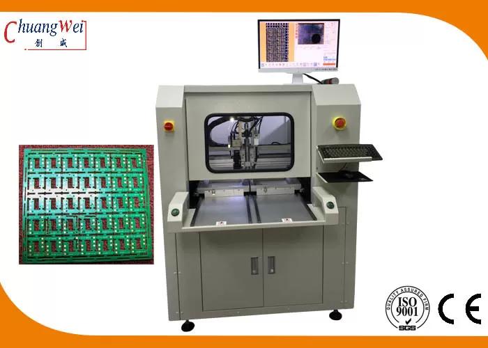
It is a stand alone router machine specially designed to route (depanelize) printed circuit board assemblies (PCBA) into individual assemblies. The machine can accomodate larger PCBs in its two table configuration with maximum panel size of 650mm x 5

Used SMT Equipment | Pick and Place/Feeders
Used, Universal Instruments 49889215 DL-60 Plus 8mm Dual Lane Gold Feeders.Price listed is for a quantity of ONE, sold used, as is, as pictured, visually inspected to be completed & functional prior to shipping.* Quantity Discount available for 5 or

Used SMT Equipment | Pick and Place/Feeders
Used, Universal Instruments 49889215 DL-60 Plus 8mm Dual Lane Gold Feeders over 200 in stock.Price listed is for a quantity of ONE, sold used, as is, as pictured, visually inspected to be completed & functional prior to shipping. CONTACT: AssuredTech
Industry News | 2017-04-11 21:19:32.0
GPD Global offers versatile large format inline dispensing systems and stand-alone liquid dispense technologies for maximizing product yield. This is the largest standard PCB dispensing system platform in the industry.
Industry News | 2013-10-10 09:56:45.0
GPD Global has again pushed the limits for small-volume dispensing with its new Nano-Piston pump. Dots of conductive adhesive down to 100 μm and solder paste for 01005s are possible with the Nano-Piston Pump.
Technical Library | 2019-10-10 00:26:28.0
Voids are a plague to our electronics and must be eliminated! Over the last few years we have studied voiding in solder joints and published three technical papers on methods to "Fill the Void." This paper is part four of this series. The focus of this work is to mitigate voids for via in pad circuit board designs. Via holes in Quad Flat No-Lead (QFN) thermal pads create voiding issues. Gasses can come out of via holes and rise into the solder joint creating voids. Solder can also flow down into the via holes creating gaps in the solder joint. One method of preventing this is via plugging. Via holes can be plugged, capped, or left open. These via plugging options were compared and contrasted to each other with respect to voiding. Another method of minimizing voiding is through solder paste stencil design. Solder paste can be printed around the via holes with gas escape routes. This prevents gasses from via holes from being trapped in the solder joint. Several stencil designs were tested and voiding performance compared and contrasted. In many cases voiding will be reduced only if a combination of mitigation strategies are used. Recommendations for combinations of via hole plugging and stencil design are given. The aim of this paper is to help the reader to "Fill the Void."
Technical Library | 2021-06-21 19:34:02.0
In this era of electronics miniaturization, high yield and low-cost integrated circuit (IC) substrates play a crucial role by providing a reliable method of high density interconnection of chip to board. In order to maximize substrate real-estate, the distance between Cu traces also known as line and space (L/S) should be minimized. Typical PCB technology consists of L/S larger than 40 µ whereas more advanced wafer level technology currently sits at or around 2 µm L/S. In the past decade, the chip size has decreased significantly along with the L/S on the substrate. The decreasing chip scales and smaller L/S distances has created unique challenges for both printed circuit board (PCB) industry and the semiconductor industry. Fan-out panel-level packaging (FOPLP) is a new manufacturing technology that seeks to bring the PCB world and IC/semiconductor world even closer. While FOPLP is still an emerging technology, the amount of high-volume production in this market space provide a financial incentive to develop innovative solutions in order to enable its ramp up. The most important performance aspect of the fine line plating in this market space is plating uniformity or planarity. Plating uniformity, trace/via top planarity, which measures how flat the top of the traces and vias are a few major features. This is especially important in multilayer processing, as nonuniformity on a lower layer can be transferred to successive layers, disrupting the device design with catastrophic consequences such as short circuits. Additionally, a non-planar surface could also result in signal transmission loss by distortion of the connecting points, like vias and traces. Therefore, plating solutions that provide a uniform, planar profile without any special post treatment are quite desirable.

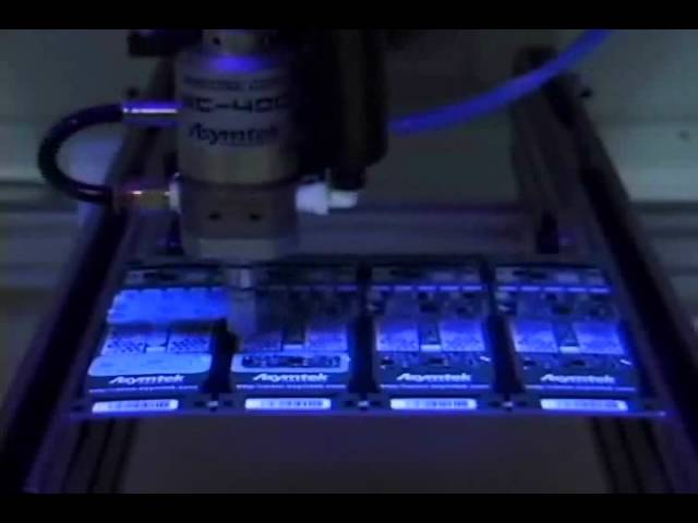
PV inverters require reliability against ingress humidity and dust in harsh environments, like deserts. Conformal coating is critical to protect inverter PCBA. Shown with the SC-400. http://www.nordsonasymtek.com
Training Courses | | | PCB Rework and Hand Soldering Courses
The PCB rework and hand soldering courses courses cover techniques of rework and repair of PCBs, BGAs and other electronics assemblies, and teach fundamentals of soldering of electronics assemblies.
Training Courses | | | PCB Rework and Hand Soldering Courses
The PCB rework and hand soldering courses courses cover techniques of rework and repair of PCBs, BGAs and other electronics assemblies, and teach fundamentals of soldering of electronics assemblies.
Events Calendar | Wed Oct 20 18:30:00 UTC 2021 - Wed Oct 20 18:30:00 UTC 2021 | ,
Great Lakes Chapter Webinar: Low Melting Alloy & Selection of the Right Chemistry for Reliability
ASYMTEK Products | Nordson Electronics Solutions | https://www.nordson.com/en/divisions/dage/about/news/nordson-advanced-technology-kk-japan-moves-to-larger-customer-focused-facility
Nordson Advanced Technology KK Japan Moves to Larger Customer Focused Facility X-Ray Inspection and Test Products Corporate | Global Directory | Languages Division Only All of Nordson Home Products Bondtesting Systems Micro Materials Testing Wafer Inspection and Metrology X-ray Inspection Systems X-ray Counting Systems Applications Battery
PCB Libraries, Inc. | https://www.pcblibraries.com/Forum/hole-size-for-through-hole-compoent_topic3025_post12054.html
. I am asking about drilled hole size. The IPC recommendation says Minimum hole size. Tom H Members Profile Send Private Message Find Members Posts Add to Buddy List Admin Group Joined
.jpg)
.jpg)