We manufacture multi PCB up to 12 layer,The details of our capabilities:*Micro fine line to 4 mil *Blind & buried via hole *Flying-probe testing *Carbonlack *FR4 thickness: 0.3/0.4/0.8/1.0/1.2/1.5/2.0/2.4/3.2mm *Small quantities are available *Golden finger *HAL & chemical tin
Industry Directory | Manufacturer
UWELLPCB.com is the PCB supplier. We offer PCB from single side board, double side PCB to 32layer board,including the Rigid PCB, Flex PCB, Rigid-flex PCB,Quick-turn prototype and PCB assembly
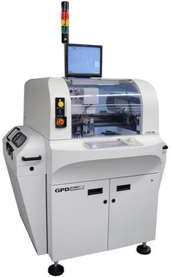
High Precision Dispensers - MAX Series (Non-Heated) Max Series is capable of a wide variety of dispense applications including MicroVolume, Solder Paste and Conductive Adhesive, Underfill, Surface Mount Adhesive, Dam and Fill, Encapsulations, LED En
New Equipment | Cleaning Equipment
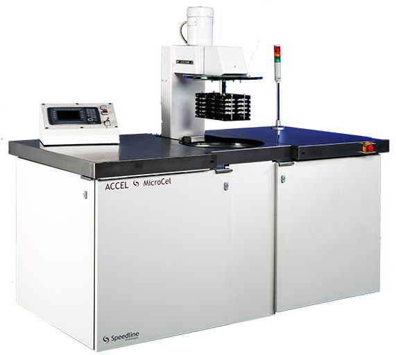
The first technology to use centrifugal energy to clean electronic circuit assemblies, precision parts, and semiconductor packages. The system offers unparalleled penetration, solubilization, and contaminant removal The MicroCel Centrifugal Cleanin
Electronics Forum | Fri Jul 30 14:16:11 EDT 2004 | C.W
For VIA In PAD design, what's the difference between a thru vias and a blind via? thanks' chester
Electronics Forum | Fri Jul 30 14:21:36 EDT 2004 | C.W
what's the difference between a thru vias and a blind via?
Used SMT Equipment | AOI / Automated Optical Inspection
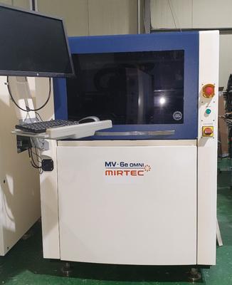
Non-blind spot digital 8 projection moiré 3D inspection technology Inspection for diffuse reflection component, OCR, micro crack precisely by 8 phases coaxial color lighting Smallest componentinspection by ultra-high resolution camer
Used SMT Equipment | Pick and Place/Feeders
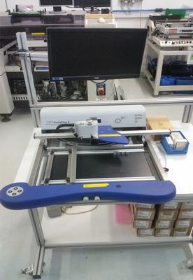
PROTOPLACE S - SEMI-AUTOMATIC SMT ASSEMBLY SYSTEM DESCRIPTION: SMT Pick & Place of PCB Prototypes The LPKF ProtoPlace S is an ergonomically designed, semi-automatic pick & place system for the professional assembly of SMT printed circuit board protot
Industry News | 2011-09-21 12:11:34.0
GPD Global will showcase its Positive Cavity Displacement (PCD) 'H' Series high resolution pumps in Booth #133 at the upcoming SMTA International Conference & Exhibition.
Industry News | 2011-09-12 12:04:25.0
GPD Global will showcase its Positive Cavity Displacement (PCD) 'H' Series high-resolution pumps in Booth #439 at the upcoming IMAPS 44th International Symposium on Microelectronics

Parts & Supplies | Circuit Board Assembly Products
1). 80 *190mm/2up, FR-4 2). 6 layers at 1.4mm thick 3). 35 μm copper weight 4). Green solder mask LPI/White legend 5). ENIG surface finish 6). Blind via from Layer 1 to layer 2 7). Via in pad plugged conductive resin
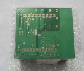
Parts & Supplies | Circuit Board Assembly Products
1). 100mm x 98mm/1up, FR-4, 2). 1mm +/-0.1mm,6 Layers 3). 1oz copper finished 3). Green solder mask/white legend 4). Min. hole 0.15mm, 4/4 mil track/gap 5). Blind via layer 1-2, via-in-pad. 6). Immersion gold surface finish
Technical Library | 2019-07-17 17:56:34.0
The increased demand for electronic devices in recent years has led to an extensive research in the field to meet the requirements of the industry. Electrolytic copper has been an important technology in the fabrication of PCBs and semiconductors. Aqueous sulfuric acid baths are explored for filling or building up with copper structures like blind micro vias (BMV), trenches, through holes (TH), and pillar bumps. As circuit miniaturization continues, developing a process that simultaneously fills vias and plates TH with various sizes and aspect ratios, while minimizing the surface copper thickness is critical. Filling BMV and plating TH at the same time, presents great difficulties for the PCB manufactures. The conventional copper plating processes that provide good via fill and leveling of the deposit tend to worsen the throwing power (TP) of the electroplating bath. TP is defined as the ratio of the deposit copper thickness in the center of the through hole to its thickness at the surface. In this paper an optimization of recently developed innovative, one step acid copper plating technology for filling vias with a minimal surface thickness and plating through holes is presented.
Technical Library | 2023-01-10 20:15:42.0
Over the past years there has been consistent growth in the use of electroless nickel / immersion gold (ENIG) as a final finish. The finish is now frequently being used for PBGA, CSP, QFP and COB and more recently gathered considerable interest as a low cost under-bump metallization for flip chip bumping application. One of the largest users for this finish has been the telecommunication industry, were millions of square meters of PCBs with ENIG have been successfully used. The nickel layer offers advantages such as multiple soldering cycles and hand reworks without copper dissolution being a factor. The nickel also acts as a reinforcement to improve through-hole and blind micro via thermal integrity. In addition the nickel layer offers advantages such as co-planarity, Al-wire bondability and the use as contact surface for keypads or contact switching. Especially those pads, which are not covered by solder need a protective coating in corrosive environment – such as high humidity or pollutant gas.
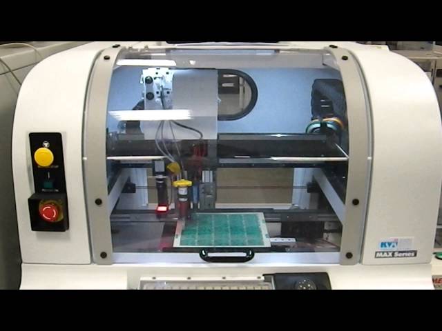
High Precision Dispensers - MAX Series (Non-Heated) Max Series is capable of a wide variety of dispense applications including MicroVolume, Solder Paste and Conductive Adhesive, Underfill, Surface Mount Adhesive, Dam and Fill, Encapsulations, LED En
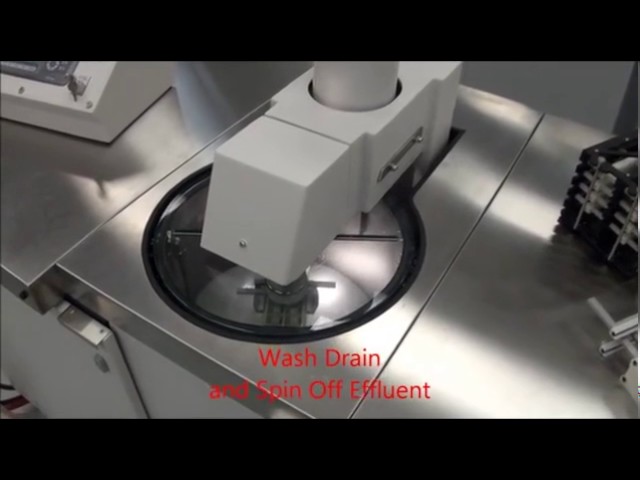
The first technology to use centrifugal energy to clean electronic circuit assemblies, precision parts, and semiconductor packages. The system offers unparalleled penetration, solubilization, and contaminant removal The MicroCel Centrifugal Cleanin
Training Courses | | | IPC-6012 Specialist (CIS)
The Certified IPC-6012 Specialist (CIS) training covers design, fabrication and inspection of rigid printed boards.
Training Courses | | | IPC-6012 Trainer (CIT)
The Certified IPC-6012 Trainer (CIT) courses recognize individuals as qualified trainers in the area of design, fabrication and inspection of rigid printed boards and prepare them to deliver Certified IPC-6012 Specialist (CIS) training.
Events Calendar | Mon Apr 23 00:00:00 EDT 2018 - Thu Apr 26 00:00:00 EDT 2018 | Shanghai, China
SMTA China East Conference 2018
Career Center | Dana Point, California USA | Sales/Marketing
We are currently seeking sales reps nationwide for this rapidly growing supplier of printed circuit boards (since 1986)with facilities in southern CA and eight PCB facilities in China and Taiwan, all ISO 9002 certified and UL94V-0 approved, some are
Career Center | Erode, Tamilnadu India | Engineering
Professional Summary 3+ years of experience in the PCB CAM engineering Exposure to FRONTLINE GENESIS 2000 Having exposure in UCAM Exposure to Create, Array & Panelize it for manufacturability Experienced in Creating impedance cou
SMTnet Express, July 18, 2019, Subscribers: 32,162, Companies: 10,836, Users: 24,951 Via Fill and Through Hole Plating Process with Enhanced TH Microdistribution Credits: MacDermid Inc. The increased demand for electronic devices in recent years
ASYMTEK Products | Nordson Electronics Solutions | https://www.nordson.com/en/divisions/dage/products/micro-materials-tester?con=t&page=10
Micro Materials Tester | Nordson DAGE X-Ray Inspection and Test Products Corporate | Global Directory | Languages Division Only All of Nordson Home Products Bondtesting Systems Micro Materials Testing Wafer Inspection and Metrology X-ray Inspection Systems X-ray Counting Systems Applications Battery
Imagineering, Inc. | https://www.pcbnet.com/capabilities/fabrication/hdi/
. Our micro via formation technology uses lasers to drill micro vias, also called blind via-holes (BVHs). With the ability to place on or off the pads, these holes let you selectively create routing room in denser parts of the substrate


