Industry Directory | Distributor / Manufacturer / Manufacturer's Representative
A distributor of high quality surface mount and related production equipment. Currently distribute Mirae Placement, SJ Inno Tech Printers, and Xavis X-Ray.
Qualification of boards and assemblies is the comparison of the board or assembly to an industry standard. Specifically, we qualify printed circuit boards to IPC-6012 – Qualification and Performance Specifications for Rigid Printed Boards and
New Equipment | Component Counters / SMD Counters
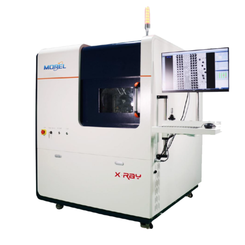
S-7200 X-Ray Inspection System Machine X-ray detection equipment is a very advanced detection technology, which can detect the internal structure and contact surface of objects. X-ray inspection equipment can be used to detect the structure of solde
Electronics Forum | Wed Aug 19 05:01:38 EDT 2020 | toki
@DWL it will be used as inspection tool for process validation. Thanks for the suggestions.
Electronics Forum | Tue Aug 18 17:27:28 EDT 2020 | cyber_wolf
@ Wellman Rau Please slither somewhere else. This is a technical forum.
Industry News | 2012-01-23 00:02:12.0
MIRTEC, “The Global Leader in Inspection Technology”, will premier its complete line of 3D AOI, SPI, X-ray and LED inspection systems at the IPC APEX Expo in booth #3637.
Industry News | 2003-05-22 08:54:17.0
Allows PCA Manufacturers to Compare Costs of Alternative Test Strategies
Technical Library | 2019-05-24 09:27:33.0
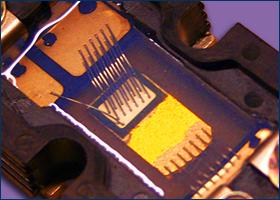
Decapsulation, or de-cap, is a failure analysis technique which involves the removal of material packaging from an integrated circuit (IC). After de-cap, visual inspection by optical microscopy of the internal circuitry may reveal areas where damage is most likely to have occurred. In addition, scanning electron microscopy (SEM) with energy dispersive x-ray spectroscopy (EDS) can identify the composition of any anomalies present after de-cap under higher magnification. The removal process of package material can be done either mechanically or chemically depending on the design of the integrated circuit. With ceramic packaging, de-cap is usually done mechanically by chiseling off the top with a fine razor and small hammer. For plastic packaging, de-cap requires chemical etching by strong acids. In this Tech Tips article, de-cap by chemical etching will be outlined step by step.
Technical Library | 2019-05-29 10:38:59.0
Decapsulation, or de-cap, is a failure analysis technique which involves the removal of material packaging from an integrated circuit (IC). After de-cap, visual inspection by optical microscopy of the internal circuitry may reveal areas where damage is most likely to have occurred. In addition, scanning electron microscopy (SEM) with energy dispersive x-ray spectroscopy (EDS) can identify the composition of any anomalies present after de-cap under higher magnification. The removal process of package material can be done either mechanically or chemically depending on the design of the integrated circuit. With ceramic packaging, de-cap is usually done mechanically by chiseling off the top with a fine razor and small hammer. For plastic packaging, de-cap requires chemical etching by strong acids. In this Tech Tips article, de-cap by chemical etching will be outlined step by step.

ACI Technologies Inc. (ACI) is a scientific research corporation dedicated to the advancement of electronics manufacturing processes and materials for The Department of Defense and industry. This video provides an overview of our commercial service

Welcome to this Defect of the Month video on head in and on pillow, this series of videos were produced for and featured as part of the NPL/IPC video library and examples are taken from the NPL Defect Database. Over the last couple of years there hav
Training Courses | | | PCB Assembly Courses
The PCB assembly courses provide knowledge of different processes and equipment used in TH and SMT assembly of printed circuit boards.
Training Courses | | | PCB Rework and Hand Soldering Courses
The PCB rework and hand soldering courses courses cover techniques of rework and repair of PCBs, BGAs and other electronics assemblies, and teach fundamentals of soldering of electronics assemblies.
Events Calendar | Tue Feb 12 00:00:00 EST 2019 - Tue Feb 12 00:00:00 EST 2019 | ,
Webinar: BGA and Area Array Process Defects - Causes & Cures
Events Calendar | Wed Dec 06 00:00:00 EST 2017 - Wed Dec 13 00:00:00 EST 2017 | Rolling Meadows, Illinois USA
X-Ray of PCBs Webtorial
Career Center | , Israel | Engineering,Maintenance,Technical Support
I was born on June , 1972 in Khmelnitsky city , Ukraine . I am male. From 1979 to 1987 I was studying at secondary school #7, having finished which I entered the Technical College of Khmelnitsky in specialty Machine Tools with Computer Numeric Contr
Career Center | la jolla, California USA | Engineering
More than 18 years experience in AOI. Refer to my resume for more details.
's innovative X-ray systems; Glenbrook Technologies
Featured Article Return to Front Page Industrial X-Ra
Imagineering, Inc. | https://www.pcbnet.com/blog/when-to-use-x-ray-inspection-in-pcbs/
? Instead of disassembling the component, X-ray inspection allows manufacturers to monitor PCB quality without damaging or deconstructing the circuit board
Baja Bid | https://bajabid.com/product/focalspot-nxr-1525-x-ray-inspection-system/
FocalSpot NXR-1525 X-Ray Inspection System - Baja Bid LLC Skip to content Your EMS Asset Management Partner Careers | Current Auctions Linkedin page opens in new window Baja Bid LLC Your EMS Asset Management Partner Home About Services Managed Online Auctions Asset Analysis Consignment Program Cash Buyout Program

Our Company handle AOI (Auto Optical Inspection) and SPI (Solder Paste Inspection) Machines.
Equipment Dealer / Broker / Auctions
Hwaseong-si, Gyeonggi-do, Korea
Hwaseong-si, South Korea
Phone: +82-1029254936


