
Industry Directory | Consultant / Service Provider / Media / Publisher / Online Resource / Other
PCB Libraries' "Footprint Expert" suite uses CAD LEAP(tm) Technology to greatly simplify footprint and 3D STEP model creation; it is used by tens of thousands of PCB designers and engineers all over the world.
A minority owned business with 40 plus years of experience that can fit your needs, in electrical engineering, printed circuit board, and mechanical design. With Alta Design Corp, we want to be an extension of your company. We understand the meaning of �Time to Market� and will ensure we meet your due date, while being price competitive.
Panasonic NPM Modular SMT Chip Mounter Machine Product name Panasonic NPM SMT Chip Mounter Model NPM-D3 NPM-W2 NPM-TT2 NPM-W2S Concept Dual-gantry, multi-head, process-driven module Dual-gantry,
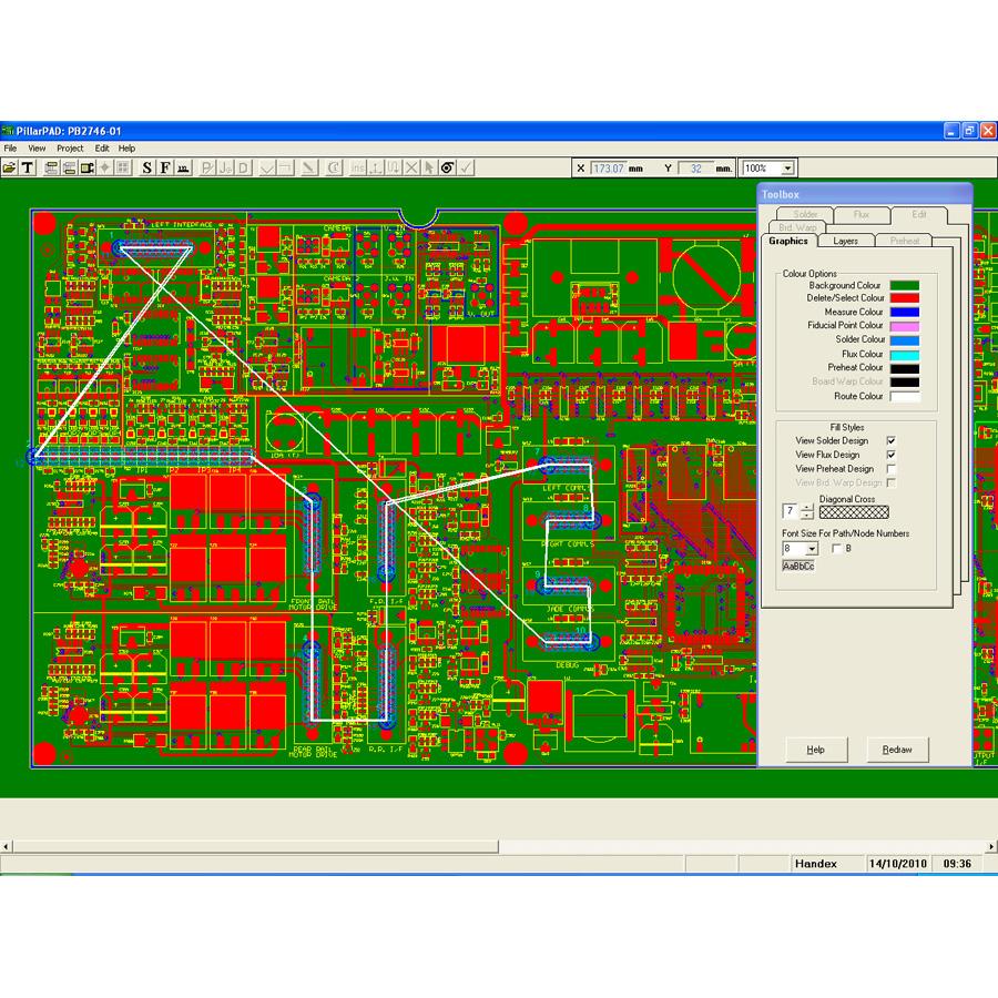
An offline process programming system Allows easy creation of flux, pre-heat and solder joints and baths Produces graphical representations of the PCB Solder nozzles shown as actual size Uses industry standard Gerber Data 90% of the programmin
Electronics Forum | Fri Nov 27 00:36:02 EST 2015 | slouis2014
I just encountered a BGA design were in, underneath the BGA is a silkscreen that covered the entire bottom of the component except for the copper pads. Can you give any information and advice for this type of design.
Electronics Forum | Fri Dec 20 09:01:27 EST 2002 | russ
Greetings, Does anybody out there have any experience with 0306 capacitors (not 0603). I am trying to find a pad design for this component. I have searched the archives to no avail. The component is .06 long by .03 wide with .007" solder terminat
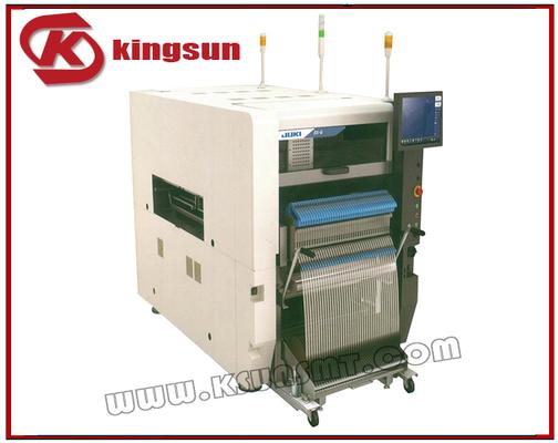
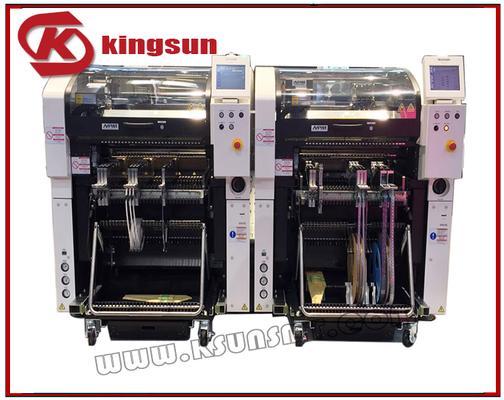
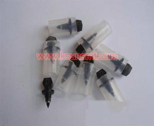
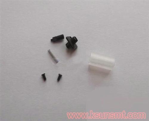
Used SMT Equipment | Pick and Place/Feeders
Product number: RX - 6 Detailed product introduction Characteristic: With high productivity, versatility, highquality new modular placement machine RX - 6 listed Draw/monitor corresponding patch Components in speed Chip components: 42000 CPH *
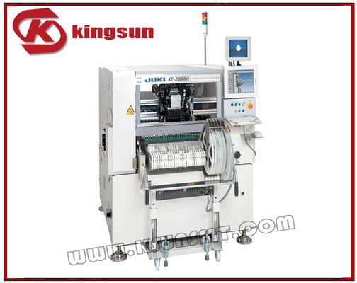
Used SMT Equipment | Pick and Place/Feeders
Product name: KE - 2080 JUKI high-speed chipmounter Product number: KE - 2080 Detailed product introduction Characteristic: Small components of high speed SMT capacityand IC or complex shape abnormity components of high precision SMT ability andg
Industry News | 2003-06-17 08:07:40.0
The Radiall SMT coupler range now includes the new 14.2 x 5.1mm mini type.
Industry News | 2003-04-29 08:27:33.0
Emerson Energy Systems is using Weidmuller's Minimate S2L/B2L PCB connector for its IMT 2000 multifunction unit, thanks to its space saving design and competitive price.
Parts & Supplies | SMT Equipment
YAMAHA NOZZLE SERIES Brand Model Specification Material of nozzle tip YAMAHA YV100II 31#NOZZLE 0402 / 0603 / 0805 (X) Tungsten steel YAMAHA YV100II 31#NOZZLE 0402 / 0603 / 0805 (X) Diamond steel YAMAHA YV100II 32#NOZZLE For IC of tiny size Tun
Parts & Supplies | SMT Equipment
YAMAHA NOZZLE SERIES Brand Model Specification Material of nozzle tip YAMAHA YV100II 31#NOZZLE 0402 / 0603 / 0805 (X) Tungsten steel YAMAHA YV100II 31#NOZZLE 0402 / 0603 / 0805 (X) Diamond steel YAMAHA YV100II 32#NOZZLE For IC of tiny size Tun
Technical Library | 2020-05-08 18:22:31.0
A customer contacted the Helpline to perform analysis on a lead-free assembly which exhibited intermittent functionality. The lead-free assembly exhibiting intermittent functionality when pressure was applied to the ball grid array (BGA) packages. Industrial adaptation of a Restriction of Hazardous Substances (RoHS) compliant solder standard has created a new host of failure modes observed in lead-free assemblies. Pad cratering occurs when fractures propagate along the epoxy resin layer on the underside of the BGA connecting pads. While originating from process, design, and end use conditions, it is the combination of a rigid lead-free solder with inflexible printed circuit board (PCB) laminates that has advanced the prevalence of this condition. Pad cratering is simply the result of mechanical stress exceeding material limitations.
Technical Library | 2019-05-29 01:47:22.0
1.Vias near SMD pads: Solder can flow into the via after melted. As a result cold joint will appear in the end. Check the picture below. 2.Vias on SMD pads: Solder can flow into the via more easier after melted. Check the picture below. 3.Via opening without soldermask covered. When workers solder TH parts by hand, soldering iron can touch vias sometime, then tiny amounts molten solder will stay on vias. This can lead to electrical short easily. We recommend you make all vias tenting (covered by solder mask) if it is possible.
PCBNPI-Professional PCB Fab/PCB Assembly Service Provider From China

www.unisoft-cim.com/pcbtest.htm - In minutes the Unisoft ProntoTEST-FIXTURE software translates CAD & BOM files into real reference designators, netlists, X/Y component pin geometries, values, tolerances, part numbers, etc. This data is used by Test

The PCB Footprint Expert is a powerful CAD library development tool powered by our own proprietary CAD LEAP Technology (Libraries Enhanced with Automated Preferences). It is packed with very powerful advanced library management features that cuts foo
Training Courses | | | PCB Rework and Hand Soldering Courses
The PCB rework and hand soldering courses courses cover techniques of rework and repair of PCBs, BGAs and other electronics assemblies, and teach fundamentals of soldering of electronics assemblies.
Training Courses | | | PCB Rework and Hand Soldering Courses
The PCB rework and hand soldering courses courses cover techniques of rework and repair of PCBs, BGAs and other electronics assemblies, and teach fundamentals of soldering of electronics assemblies.
Events Calendar | Thu Oct 03 00:00:00 EDT 2019 - Thu Oct 03 00:00:00 EDT 2019 | ,
IPC Tech Ed Webinar Series: Ball Grid Array (BGA) and Bottom Termination Component (BTC) Design and Assembly Challenges: Reflow Profiling to Achieve Low Defect Rates and Successful Assembly! – Part 2
Events Calendar | Wed Apr 20 00:00:00 EDT 2022 - Wed Apr 20 00:00:00 EDT 2022 | ,
Virtual Course: Selection Criteria of Surface Finish for Next Generation PCB Technologies
Career Center | Sherman, Texas USA | Engineering,Production,Research and Development,Technical Support
SMT Packaging Engineer: Location: Texas - Sherman , TX Group: HVAL Degree Requirements: BS ME/ChemE/Materials The person in this position will have the ability to make very significant financial contributions to TI because this is a very critic
Career Center | Lincoln, Nebraska USA | Engineering
Brief Description of Job Duties: Provide new program engineering support with emphasis on technical SMT process development. Key activities would include recommendations and implementation of components, SMT pad design, solder methods, testing and r
Career Center | Newport Beach, California USA | Engineering,Management,Production
KEVIN RAGER P.O.BOX 7878, NEWPORT BEACH, 949 922 8997, KEVIN.RAGER@EDA-INC.US OBJECTIVE I am trying to find a consistent work flow that provides mentally challenging yet stimulating experiences in design and prototype development. EXPERIENCE 1997
PCB Libraries, Inc. | https://www.pcblibraries.com/forum/design-smt-pad-for-magnet-wire_topic1206.html
Design SMT pad for magnet wire - PCB Libraries Forum Forum Home > PCB Footprint Expert > Questions & Answers New Posts FAQ Search Events Register Login Design SMT pad for magnet wire
Imagineering, Inc. | https://www.pcbnet.com/blog/considerations-for-pcb-board-design-layout/
Considerations for PCB Board Design & Layout | Imagineering, Inc. Skip to main content Resources Support Contact Us FAQs Live Chat My Account 847-806-0003 Menu PCB Capabilities Fabrication Technology Roadmap Materials Available HDI Tolerances Certifications


