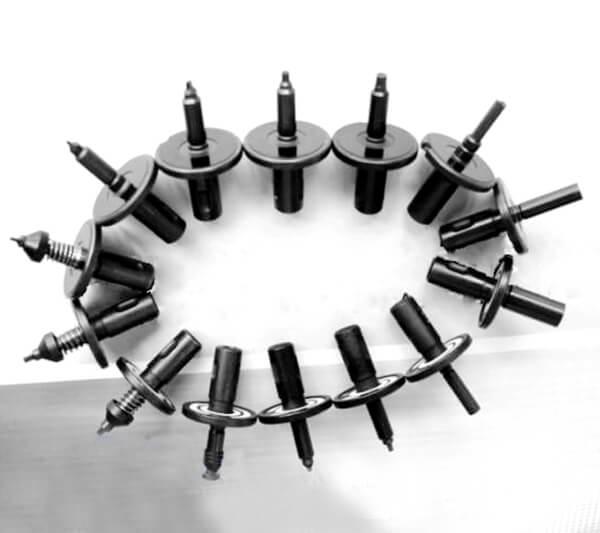
http://www.flason-smt.com/product/I-Pulse-Nozzle-for-M1-M2-and-M4.html I-Pulse Nozzle for M1 M2 & M4 SMT Nozzle I-Pulse Nozzle I-Pulse Nozzle for M1 M2 & M4 Usage:I-Pulse pick and place machine Product description: I-Pulse Nozzle for
Samsung FW-1 Tray Feeder for Samsung CP series SMT Feeder Samsung FW-1 Tray Feeder for Samsung CP series Samsung Feeder Pick and Place Machine Feeder Product description: Samsung FW-1 Tray Feeder for Samsung CP series INQUIRY Sams
Electronics Forum | Wed May 09 01:23:17 EDT 2001 | GregH
Hi, My Bottomside component pads are 1:1 with my topside land sizes/dimensions. I have difficulties catching solders on my bottomside smd chips (SMB Diodes, 0805 RC Chips). What should the bottomside components for wave soldering be greater than my t
Electronics Forum | Wed May 09 10:40:10 EDT 2001 | davef
First, your primary side component pads should be designed according to SM-782A, "Surface Mount design & Land Pattern Standard". Next if you did that and your secondary side component pads are the same size as your primary side components, your diff
Industry News | 2019-11-05 22:07:01.0
Tenting a via refers to covering via with soldermask to enclose or skin over the opening. A via is a hole drilled into the PCB that allows multiple layers on the PCB to be connected to each other. A non tented via is just a via that is not covered with the soldermask layer. Leaving these vias exposed or covered has pros and cons depending on the your design and manufacturing requirements.
| https://www.smtfactory.com/Hot-Air-8-Trays-Electric-Reflow-Convection-Oven-with-High-Quality-pd48530624.html
Reflow Wave Oven Reflow Oven Smd Smt Reflow Soldering Oven Reflow Oven Heating Reflow Oven Mini Smt Reflow Oven Reflow Oven Nitrogen Reflow Oven Desktop Reflow Oven Heating Element Reflow Oven
| http://etasmt.com/te_news_industry/2019-06-13/6961.chtml
. Reflow soldering machine: refers to soldering a solder paste previously coated on a pad by heating to electrically interconnect the leads or solder terminals of the electronic components pre-applied on the pads and the pads on the pcb

.gif)


