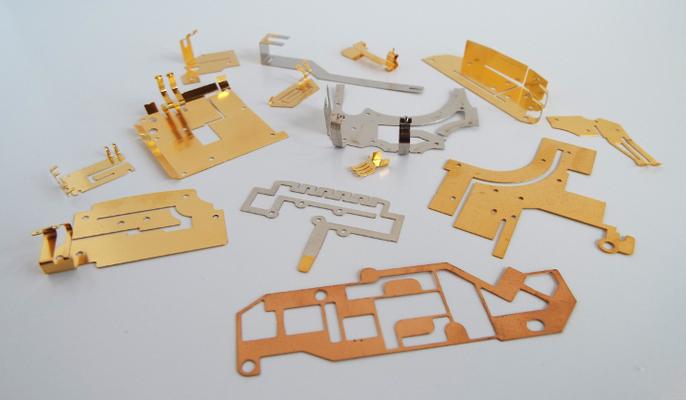
Datum Alloys is an international supplier of speciality metals and special purpose alloys,
Antennas exist in all communication equipment and in a broad range of electronics. The industries that use antennas range from telecom to medical industry to military applications. Current antennas are much smaller than previous generations and, in m
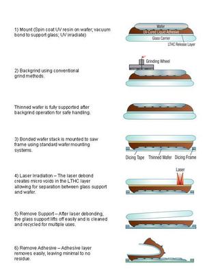
The 3M Wafer Support SystemTM provides a temporary bonding solution to support wafers during conventional thinning operations as well as post thinning operations. The 3M UV curable adhesive is spun on the wafer surface and is used as a bonding agent
Electronics Forum | Mon Jul 16 16:39:17 EDT 2007 | davef
We doubt that entrapped process chemicals cause under-etch. Over-etch maybe, but not under-etch Under-etch is an indicator of improper process control/improper chemistry during etching. Under-etch can result in bridging between traces, resulting in
Electronics Forum | Thu Jan 10 11:22:48 EST 2013 | pbarton
Looks to me like under etching of the underlying copper and the gold is just plated to all of the exposed copper surface. Is this characteristic the same on all solderable pads? You will not be able to remove this gold.
Industry News | 2003-03-12 08:28:44.0
CAM350 Release 8 is aimed at allowing engineering and manufacturing groups to detect and fix potential PCB fabrication problems earlier in the process.
Industry News | 2013-07-31 07:28:30.0
Today, the electronics manufacturing industry’s first design guidelines for printed electronics, IPC/JPCA-2291, Design Guidelines for Printed Electronics, was released by IPC — Association Connecting Electronics Industries® and JPCA.
Technical Library | 2019-05-24 09:27:33.0
Decapsulation, or de-cap, is a failure analysis technique which involves the removal of material packaging from an integrated circuit (IC). After de-cap, visual inspection by optical microscopy of the internal circuitry may reveal areas where damage is most likely to have occurred. In addition, scanning electron microscopy (SEM) with energy dispersive x-ray spectroscopy (EDS) can identify the composition of any anomalies present after de-cap under higher magnification. The removal process of package material can be done either mechanically or chemically depending on the design of the integrated circuit. With ceramic packaging, de-cap is usually done mechanically by chiseling off the top with a fine razor and small hammer. For plastic packaging, de-cap requires chemical etching by strong acids. In this Tech Tips article, de-cap by chemical etching will be outlined step by step.
Technical Library | 2019-05-29 10:38:59.0
Decapsulation, or de-cap, is a failure analysis technique which involves the removal of material packaging from an integrated circuit (IC). After de-cap, visual inspection by optical microscopy of the internal circuitry may reveal areas where damage is most likely to have occurred. In addition, scanning electron microscopy (SEM) with energy dispersive x-ray spectroscopy (EDS) can identify the composition of any anomalies present after de-cap under higher magnification. The removal process of package material can be done either mechanically or chemically depending on the design of the integrated circuit. With ceramic packaging, de-cap is usually done mechanically by chiseling off the top with a fine razor and small hammer. For plastic packaging, de-cap requires chemical etching by strong acids. In this Tech Tips article, de-cap by chemical etching will be outlined step by step.

Atmospheric plasma treatment is a unique technology for surface treatment in electronic assembly: nano cleaning, surface activation, and plasma coating of almost all materials – composites, plastics, metals, glass, cardboard, textiles, etc. With ANDA
355nm 10W /15W High-Precision CCD FPC/PCB UV Laser Cutting Machine With Perfect CAM interface, it supports the mainstream of the drilling and milling file format; man-machine interface is friendly; optical path is sealed, and it also has stable an
ASYMTEK Products | Nordson Electronics Solutions | https://www.nordson.com/en/divisions/march/about-us/legal/terms-and-conditions
. Standard Nordson MARCH Acceptance Criteria are outlined as follows: (VIA-Series, PCB-Series) For printed circuit board (PCB) applications, equipment uniformity and etch rate will be determined by standards and procedures outlined in Vacuum Plasma Desmear Uniformity Measurement for Rigid and Flex Printed Circuit Boards
| http://www.thebranfordgroup.com/dnn3/Auction/TSLE0523.aspx
Höllmüller LPI Developer with flexible transport Pill Pre-Clean Mec Etch Bond for paint + inner layers Höllmüller Anti-Tarnish for inner layers Mec Laif Shadow Line - Direct Metallization Laif Resist Stripper with cyclone Schmid Tin Stripper Laif Ni/Au manual electroplating w/post-cleaning + dryer Laif Ni/Au – chem


