New Equipment | Component Programming
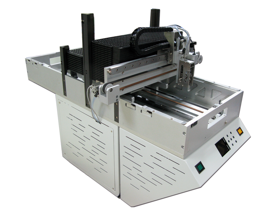
Feature Auto Tray-350 series is specifically for tray input and output, which supports 20 to 25 JEDEC standard trays. The machine can perfectly combine with DediProg's automated IC programming system and support online ink or inkjet marking. Differ
Industry Directory | Manufacturer
Intrinsiq Materials manufactures a variety of electronic ink, including screen-printable, and inkjetable copper ink, a silicon ink jet, and a nickel ink jet.
Technical Library | 2017-06-08 17:31:23.0
Recently, there has been an upsurge in efforts dedicated to developing low-cost flexible electronics by exploiting innovative materials and direct printing technologies. This interest is motivated by the need for low-cost mass-production, shapeable, and disposable devices, and the rapid prototyping of electronics and sensors. This review, following a short overview of main printing processes, reports examples of the development of flexible transducers through low-cost inkjet printing technology.
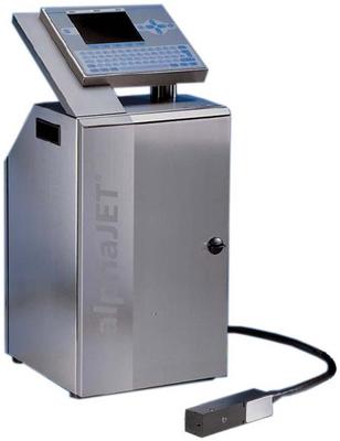
New Equipment | Cable & Wire Harness Equipment
Overview Industry proven, non-contact ink jet printers create durable, easy to read dot matrix characters on most wire and cable jackets. The programmable, non-stop wire inkjet printers automatically mark the most complex engineered harnesses at hig
Technical Library | 2018-01-11 10:48:48.0
Ink-jet printing is poised to impact the manufacturing of devices that are particularly attractive for flexible electronics, as more suitable and printable fluids become available. The addition of surfacants in the preparation of the inks usually results in additional process steps, potentially increasing cost, as well as material waste, where the surfactants also often have a negative impact on specific properties of the printed features, such as comprising electrical conductivity of metallic structures. (...)In this work, we have successfully formulated a suitable ink derived from a mixture of terpineolin cyclohexanone as a more environmentally friendly option for the exfoliation of bulk graphite, which we elaborate upon in more detail here.
Technical Library | 2018-07-03 12:27:02.0
It is becoming increasingly more important to provide a low-cost point-of-care diagnostic device with the ability to detect and monitor various biological and chemical compounds. Traditional laboratories can be time-consuming and very costly. Through the combination of well-established materials and fabrication methods, it is possible to produce devices that meet the needs of many patients, healthcare and medical professionals, and environmental specialists. Existing research has demonstrated that inkjet-printed and paper-based electrochemical sensors are suitable for this application due to advantages provided by the carefully selected materials and fabrication method. Inkjet printing provides a low cost fabrication method with incredible control over the material deposition process, while paper-based substrates enable pump-free microfluidic devices due to their natural wicking ability. Furthermore, electrochemical sensing is incredibly selective and provides accurate and repeatable quantitative results without expensive measurement equipment. By merging each of these favorable techniques and materials and continuing to innovate, the production of low-cost point-of-care sensors is certainly within reach
Technical Library | 2021-07-13 19:59:34.0
We have investigated the processing of lead-zirconate-titanate-based thick films by inkjet printing Pb (Zr0.53Ti0.47)0.98Nb0.02O3 with a 6 mol% excess of PbO nanosized powder dispersed in water. Differentwaveforms were employed to determine the optimum size and shape of the drops. A uniform, defect-free pattern with dimensions of 4 mm × 4 mm can be printed using 20 V and a drop spacing of 20 μm. The inkjet-printed films were heated to 400 °C to remove the organics and subsequently sintered at 750 and 850 °C. The correlations between the density, grain size and electromechanical properties of the thick films and bulk ceramics are qualitatively discussed. A thickness coupling factor of 46% was obtained for a 15-μm-thick film sintered at low temperature of 850 °C, which is comparable to the value of the bulk ceramic with an identical nominal chemical composition. Our results are important for the economic and environmental-benign printing of piezoelectric materials applicable in variety of electronic devices, such as sensors, actuators, transformers, piezoelectric energy harvesters and transducers.
It is not a woven product nor does it make from paper pulp. Sturdy and not easy tear. Crease-free and with sharp cutting edge Nano-technology paper treatment. Water and dust resistant. Sharp resolution displays a dynamic color and presents 3 dimensio
Industry Directory | Distributor / Manufacturer
Top 20 High-Quality PCB Fabrication and one-stop Turnkey PCB Assembly Facilities worldwide. Served national engineers for over 15 years, becoming a household name in providing full-feature multilayer PCBs engineers can trust.
Technical Library | 2020-08-13 00:59:03.0
The paper will discuss the integration of 3D printing and inkjet printing fabrication technologies for microwave and millimeter-wave applications. With the recent advancements in 3D and inkjet printing technology, achieving resolution down to 50 um, it is feasible to fabricate electronic components and antennas operating in the millimeter-wave regime. The nature of additive manufacturing allows designers to create custom components and devices for specialized applications and provides an excellent and inexpensive way of prototyping electronic designs. The combination of multiple printable materials enables the vertical integration of conductive, dielectric, and semi-conductive materials which are the fundamental components of passive and active circuit elements such as inductors, capacitors, diodes, and transistors. Also, the on-demand manner of printing can eliminate the use of subtractive fabrication processes, which are necessary for conventional microfabrication processes such as photolithography, and drastically reduce the cost and material waste of fabrication.

.gif)


