New Equipment | Assembly Services
Competitive advantages: No minimum order quantity and free sample Focus on low to medium volume production Quick and on-time delivery International approvals Great customer service Diversified shipping method Wide range of PCB supplying One

This video describes the IPC A-600 training and certification program. The IPC A-600 specification is a set of acceptability specifications for printed circuit boards. These standards determine the acceptance and reject criteria for printed wiring bo
At Barry: custom requests are common and welcome. We enjoy the challange. Extensive capabilities, wide material selection and state-of-the-art equiptment (including in-house plating and machining) ensure we can deliver a component fitting your exact
Industry News | 2019-11-05 22:08:21.0
Via in pad is the design practice of placing a via in the copper landing pad of a component. Compared to standard PCB via routing, via in pad allows a design to use smaller component pitch sizes and further reduce the PCBs overall size. With component manufactures pushing smaller parts every year and the demand from consumers for smaller devices, the usage of via in pad practices by hardware engineers have become more commonplace. In this article, we will discuss the differences between via in pad and traditional vias, when should you use via in pad, and how to design for it.

Training Courses | ON DEMAND | | IPC-600 Trainer (CIT)
The Certified IPC-600 Trainer (CIT) courses recognize individuals as qualified trainers in the area of quality assurance of bare printed circuit boards and prepare them to deliver Certified IPC-600 (CIS) training.
Industry Directory | Manufacturer
Auspi Enterprises Co., Ltd., one of the professional suppliers of printed circuits in China. We found your company info on the web knowing that you're dealing with electronics, which we think you may have demand on pcbs.

New Equipment | Assembly Services
Quick turn Prototype PCBs from 24 hour turnaround to high volume printed circuit board production from our domestic plant in USA and/or China facilities. Our Modern 38,000 sq. ft. manufacturing plant with multi-million dollar investment with latest e
New Equipment | Fabrication Services
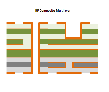
Multilayer PCB's ACI manufactures a wide variety of Multilayer PCB's for various applications spanning numerous industries and technologies. We can build your high layer count PCB's using a wide variety of high speed low loss materials from epoxies
Technical Library | 2021-09-29 13:35:21.0
In PCB circuit assemblies the trend is moving to more SMD components with finer pitch connections. The majority of the assemblies still have a small amount of through hole (THT) components. Some of them can't withstand high reflow temperatures, while others are there because of their mechanical robustness. In automotive applications these THT components are also present. Many products for cars, including steering units, radio and navigation, and air compressors also use THT technology to connect board-to-board, PCB's to metal shields or housings out of plastic or even aluminium. This is not a simple 2D plain soldering technology, as it requires handling, efficient thermal heating and handling of heavy (up to 10 kg) parts. Soldering technology becomes more 3D where connections have to be made on different levels. For this technology robots using solder wire fail because of the spattering of the flux in the wires and the long cycle time. In wave soldering using pallets the wave height is limited and pin in paste reflow is only a 2D application with space limitations. Selective soldering using dedicated plates with nozzles on the solder area is the preferred way to make these connections. All joints can be soldered in one dip resulting in short cycle times. Additional soldering on a small select nozzle can make the system even more flexible. The soldering can only be successful when there is enough thermal heat in the assembly before the solder touches the board. A forced convection preheat is a must for many applications to bring enough heat into the metal and board materials. The challenge in a dip soldering process is to get a sufficient hole fill without bridging and minimize the number of solder balls. A new cover was designed to improve the nitrogen environment. Reducing oxygen levels benefits the wetting, but increases the risk for solder balling. Previous investigations showed that solder balling can be minimized by selecting proper materials for solder resist and flux.


