Industry News | 2019-11-05 22:08:21.0
Via in pad is the design practice of placing a via in the copper landing pad of a component. Compared to standard PCB via routing, via in pad allows a design to use smaller component pitch sizes and further reduce the PCBs overall size. With component manufactures pushing smaller parts every year and the demand from consumers for smaller devices, the usage of via in pad practices by hardware engineers have become more commonplace. In this article, we will discuss the differences between via in pad and traditional vias, when should you use via in pad, and how to design for it.

Symbion P36 is an inline high-speed API solution that delivers 100% coverage for improving your product quality and boosting your productivity. Post-Paste AOI Instant Programming Easy Gerber Import 2D/3D Laser Path Superior POP™ D
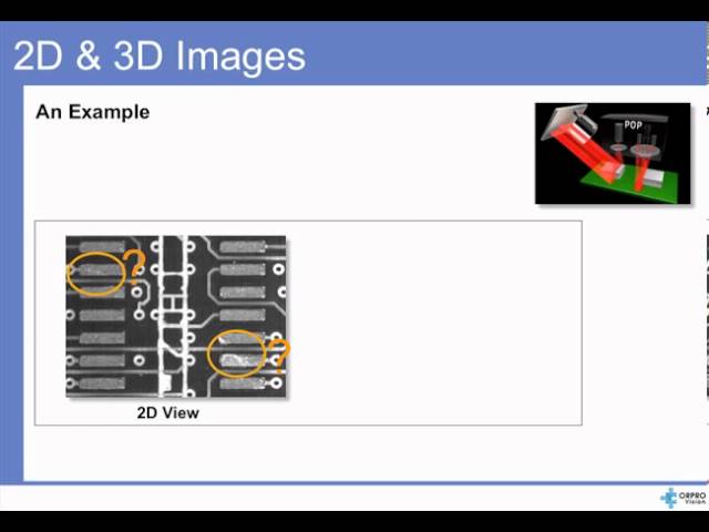
ORPRO Vision SPI Presentation. This presentation introduces the methods and technology used by ORPRO Vision in the Symbion P36 Plus SPI system. For additional information, please contact ORPRO Vision at sales.us@orprovision.com sales.eu@orprovision
Industry News | 2018-10-18 10:40:04.0
Via Tent-Holes with Solder Mask
Industry News | 2019-07-09 11:16:55.0
Thanks to Ucamco’s new Gerber Job File Editor, designers can create and edit job files that provide all essential PCB production data, including essential non-image-based information, in a standard format that can be put into an automatic production flow. Ucamco’s principal aim in doing so is to make life easier for electronics design and manufacturing professionals by facilitating clear, unequivocal communications prior to production.
Industry Directory | Consultant / Service Provider / Manufacturer
PROPOX is a manufacturer of electronics, industrial automatics, telemetric systems, tools, modules and evaluation circuits used by the constructors of electronics.
Electronics Forum | Thu Apr 22 10:57:20 EDT 1999 | Jack Coia
On various PCB's after building processes,such as reflow, flowsolder and wash. The soldermask on the PCB's have become discoloured, like a 'marble' effect all along the solder side of the board, it is lighter in contrast than normal, although when ot
Electronics Forum | Thu Apr 22 18:07:38 EDT 1999 | Tom B.
| On various PCB's after building processes,such as reflow, flowsolder and wash. The soldermask on the PCB's have become discoloured, like a 'marble' effect all along the solder side of the board, it is lighter in contrast than normal, although when
Electronics Forum | Thu Apr 22 13:20:04 EDT 1999 | Ben Kirk
| On various PCB's after building processes,such as reflow, flowsolder and wash. The soldermask on the PCB's have become discoloured, like a 'marble' effect all along the solder side of the board, it is lighter in contrast than normal, although when

.gif)

