GESP Products
SMT Products and Services offered by GESP
- SMTnet
- »
- SMT / PCB Products and Services
- »
- GESP
- »
- GESP Products
GESP Technology | 15+Years Devoted to PCB Solutions & Manufacturing »»
Headquarters: dalian, Liaoning, China

5 listed by GESP
Product |
Category |
|---|---|
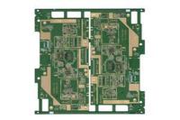
HDI PCB - HIGH DENSITY INTERCONNECT PCBsHDI circuit boards are PCBs that have a higher wiring density per unit area than regular PCBs. In general, HDI PCBs have the following features: microvias, blind and buried vias, built-up laminations. and high signal performance considerations. The evolution of PCB technology
|
|
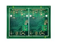
2 Layer PCB2 Layer PCB with two copper traces, also known as “Double Sided PCB” (D/S PCB). and required PTH, but it lacks buried or blind holes. Besides, Components can be constructed on both the top and bottom sides of the board. eliminating the need to worry about where to place componen...
|
|
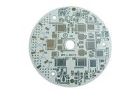
MULTILAYER PCB- UP TO 24 LAYER PCBGESP provides multilayer PCB and handle complex boards with up to 24 layers . using high-quality multilayer PCB manufacturing methods. With holes and shutters for electrical connections. these multilayer PCBs work as a single unit. Since each PCB
|
|
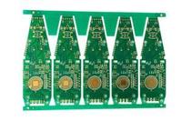
PCB PROTOTYPErototype PCBs used to test each component and find faults as early as possible. Engineers begin by reviewing testing theories and attempting to analyze the problem. Then, via testing, you can solve the design’s complexity. GESP Tech as PCB prototype manufacturer , provides simple, fa...
|
|
Quick-turn-pcb-fabricationWhen it comes to PCB fabrication, quick turn PCB is an absolute necessity. In China, we are the most premier providers of quick-turn PCB fabrication services. In the end, speed to market is a significant source of competitive advantage. GESP places...
|