|
Featured Article
|
HASL
WHAT A HASSLE, or HASL'd AGAIN by Earl Moon
INTRODUCTION
This article updates one I wrote for Printed Circuit Fabrication Magazine in December 1991. Actually, this article trashes that - and about time. I was much too kind then talking about how to control the HASL process. I really couldn't say it was uncontrollable, as no one, at that time, would have believed such an "advanced", save us all technology could be flawed. Well, it's time to dispel that bunk though some still love the stuff, and there are many staunch defenders selling equipment and process elements as well as those using its effects.
Again, I say now as then, the least controlled/controllable process in PCB manufacturing is the solder coating/hot-air-solder-leveling (HASL) process. This lack of control definitely is as due to the process itself as the boards entering it. First, solder must be "wetted" to the PCB surface and this is not a process normal to board fabrication operations as, traditionally, solder was always plated and often "fused" thereafter rendering a highly solderable surface. Second, boards received into the process often are oxidized so as not to allow acceptable solder wetting/coating.
Controllability (I now call it manageability) is important because, during the HASL process, solder must wet to all exposed metal surfaces - especially solder termination areas as SMT pads. The thing is, it doesn't well - or without quite a struggle resembling nothing manageable. Because examples of non-wetted conductors are prolific, we all know something is not right with the HASL process. That something is discussed in the following:
Figure 1 is a common example of non-wetted SMT pads. We've all seen such examples. Notwithstanding surface topography, this condition obviously is unacceptable. This is because no amount of effort or futile attempts at process management, during assembly soldering operations, allows initially acceptable solder joint quality or, of course, long-term reliability. Simply, if it doesn't wet during HASL, it won't wet during assembly. Figure 2 is an example of problems associated with this condition as a solder joint cross sectioned to show just a part of the excessive voiding effected by flux remaining in an attempt to continuing fighting excessive pad surface oxidation.
|
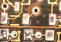
Figure 1
|
|
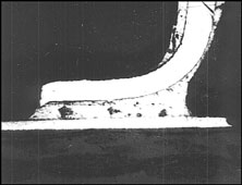
Figure 2
|
Another factor deleterious to solder joint formation and quality is excessive intermetallic compound (IMC) formation. All proponents of the process understand and admit an IMC layer is formed involving the copper surface and the eutectic solder coated onto it. Though part of any "normal" soldering process, it is formed during solder coating operations and can become too thick for subsequent assembly soldering operations to be effective. It is known that high temperature and liquid solder's intimate contact with the basis metal enhances IMC formation rate though enhance might mean too much, too quickly - as well as growth over time. Plus, after solder coating, another thermal excursion is experienced as the board travels through the hot air knives. All this adds up to a recipe for failure (created in an unmanageable process) during and after assembly operations.
It is well known that IMC is required for solder joint formation though the IMC layer itself is not a solderable surface. Therefore, say experts, there must be sufficient additional eutectic solder thickness to assure acceptable solder joint formation during assembly. Again, the conflict comes as how thick both the IMC and solder? If the IMC is too thick, and the solder is too thin (as is often the case with HASL coating), acceptable solder joints are not possible. If the IMC continues growth, becoming "extremely" thick - well, you know the outcome no matter the solder thickness. So, how much is too much and how does one control it? One doesn't.
Intermetallic compound thickness can be minimized depending on process parameters used. It is said by some that typical tin/copper IMC thickness is 6 to 12 micro-inches (.15 to .3 microns). In other hot air leveling processes, the IMC layer can exceed 100 micro-inches (2.5 microns). This is pretty contradictory and confusing stuff as "other" may mean those processes not so well managed as in different machine types and processes. That's a whole other concern because so many choices are available as vertical, horizontal, features, capabilities, cost, etc - making it hard for board shops and their customers to make "safe" decisions. How would the average board buyer begin to evaluate a board shop based on all the above?
Though difficult to measure HASL finish thickness, some findings show the range to be 80 to 1000 micro-inches (2 to 25 microns) on the same board. That's a wide range indeed. Again, this points to compromises, variables, and concerns facing all involved and affected. It comes down to how many compromises are acceptable and how each affects solder joint formation, quality, and reliability over time.
I've consulted with many operations wherein are found varying degrees of ineffective process management concerning HASL (there are none truly effective, nor can there be), and all going into it before attempting operations. Often, deleterious causes consist of poor flux management, improper or missing tools and procedures, air knives not adjusted or operating properly, solder pot dwell times and temperatures improperly set or operating, and poor control of boards introduced to the process. The latter often is the main problem as it is impossible to keep and assure copper board surfaces oxidation free. Therefore, the process often is "tweaked" mercilessly in futile attempts to overcome the main problem. This article now focuses on the process itself.
HOT AIR SOLDER LEVELING - THE PROCESS
The PCB fabrication HASL process is analog to the PCB assembly wave solder process. It requires all the same elements and sub-processes - once the process is started. I emphasize once the process is started because only a few things are fundamentally wrong with it - by itself (to be discussed). It just can't do its job mostly because of what needs processing in it.
If it weren't for often found non-wetting and excessive intermetallic compound (IMC) formations, the process, and the product effected in it, would almost be acceptable. The only other problem would be solder thickness and topography inconsistencies, or SMT pad (solder termination area) flatness and uniformity. We've all seen and complained about the "puddling" effects rendered, as in figure 3 below and figure 1 previous, and how they wreak havoc on fine pitch SMT stencil printing and placement operations.
|
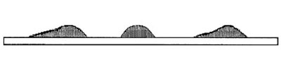
Figure 3
|
Again, the HASL process's biggest problem is what happens to boards before submission to solder leveling. This requires understanding a bit more (how much more can assemblers take) about board fabrication concerning printing, etching, and plating.
After a PCB is printed and etched (talking outers now), its surface must be coated with something to keep it from oxidizing. We all know the major reason for this is to prevent copper oxide formation. Oxides, and other contaminates, prevent solder wetting. Whatever is coated, plated, or otherwise applied to a board's conductive surfaces must keep oxidation from occurring. That's it. Otherwise, no coating is required.
Most of us know many coatings, or plating types, are available. Plating (as in electroplating), however, is the only truly effective process available to ensure contamination free copper surfaces and those effected after the process is finished. Tin/lead plating, that has been "fused" (using hot oil or convection air - though never focused IR), provides the most solderable surface yet devised. Its drawback, mimicking HASL'd surfaces, is topography. After fusing, there is a very homogeneous (very tight shiny grain structure that is very solderable) surface. However, it is one with a "dome" that can be .003" thick at its center line and no less than .001" around its edges. This, as HASL, doesn't readily invite SMT printing and placement.
Note: Some die hard advocates remind that HASL, after all, is pure eutectic solder having that advantage over tin/lead plated surfaces. To that I say, so what in light of all else negative?
I will say, that if tin/lead plated boards were HASL'd, there would be fewer solderability problems though the irregular surface condition would remain as an irritant to many, or serious problem to some. This will never happen because of associated costs and environmental issues.
Getting down to it: The pre-HASL board surface is bare copper. What's wrong with that you ask? Everything, I answer - because that surface cannot avoid becoming oxide contaminated before solder coating.
In the print and etch process, the board moves through a series of chemical solutions to final plate. This is when and where problems arise. With the specified plating thickness ensured (.001" - .0012" minimum in hole walls), the board is imaged and etched (panel plating) or the specified plating thickness is plated up along the resist walls. Walls resemble tiny canyons about .0015" high after imaging, resist polymerizing, and removal (where the conductor pattern is to be). After the imaged resist is stripped and the etching process is effected (while using tin/lead as the final etch resist), a conductor pattern is left as bare copper (after the final etch resist is stripped).
After the final tin/lead etch resist stripping operation, a final rinse is applied to the bare copper surfaces. The board can go two ways from here. In the first, it is dried, racked, and sent to HASL. The second introduces the board to a micro-etch process (usually a relatively mild acid solution to remove oxidation) followed by rinse, drying, and racking processes. In either case, drying and racking defines the problem. Boards are dried, because they cannot be introduced to HASL with wet surfaces or holes. Drying is burning, and burning is oxidation.
Note: The copper surface cleaning and micro-etch process may be carried out during the HASL process, in some machines, therefore reducing time between processes. Though more effective, a drying process still is required. This is the heart of the problem.
Depending on how long each process step takes, and how long it is before the board is introduced to solder coating, the amount of oxidation correlates directly. It matters little, however, as copper oxidizes rapidly and any amount can negatively affect the outcome.
Ok! That problem has been addressed. Now, what to do about it? There really isn't much that can be done, but an effort must be made in what remains a process very dependent on what enters it. That effort consists of what we all experience as qualified wave solder process, manufacturing support, and quality engineers - plus operators. For this, I have broken down each HASL sub-process as follows (after an overview) - keeping in mind most board shops are not soldering or solderability experts:
HASL PROCESS OVERVIEW
To effect solder coating, a board is loaded and cycled into the machine (figure 4) and process. After flux application, board preheating, and flux activation, the board is conveyed becoming totally immersed in molten solder for a specified time. To effect solder leveling, the board is conveyed out of the molten solder, through a set of air knives where hot, pressure/volume controlled air is directed at both board surfaces removing molten solder as the board passes through them. Solder is leveled, or blown off board surfaces as is hole solder.
|
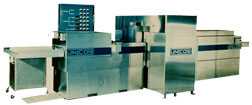
Figure 4
|
Molten solder is kept in motion as it is continuously pumped through the pot and over the weir at its surface. A high solder movement rate provides a scrubbing action over board surfaces while preventing any solder pot problems.
Critical process parameters are solder pot temperature and board dwell time during immersion. Other control factors are just as those in wave soldering.
Eutectic solder, as 63/37% tin/lead, typically is used. Its melting temperature is about 187 degrees C. However, the minimum required wetting temperature is near 220 C. with 235 C. + providing better assurance for complete wetting - depending on thermal mass and processing continuance. No matter, solder termination areas must be contamination and oxide free for any wetting to occur.
For effective process management solder temperature is maintained between 235 C. and 240 Centigrade. Within this temperature range, boards must only be subjected to solder immersion times less than 5 seconds as epoxy/glass resin system formulation Tg's typically are in the 120 C. to 180 C range. If the specified time is exceeded, thermal stress and/or shock is imparted to the board with effects as delamination, hole wall failure due to excessive Z axis expansion over extended periods, pad lifting, and associated problems. Figure 5 shows a cracked hole wall in X-Section - not a pretty picture.
|
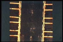
Figure 5
|
When boards are transported from the solder pot, excess solder is removed from surfaces and holes. Are knives, set to ensure correct positioning, angles, air temperatures, and air pressures and volumes, are used to "blow" away the excess leaving "acceptably leveled" surfaces and hole wall conditions. One important tradeoff may be encountered however, as it is not possible to produce a maximum surface coating thickness while maintaining specified hole diameters. Therefore, only one condition may take priority.
FLUX MANAGEMENT
Flux management, as all HASL sub-processes, must be effected just as in wave soldering. Flux must be selected for the job to be done. Usually, a mild organic type is used that may be cleaned easily in a water wash process. In some cases, in shops really out of control, new flux types are tried everyday doing to a board what shouldn't be done to anything.
All rules apply concerning flux composition and maintenance. What is specified, must be maintained. Using a standard hygrometer works to determine specific gravity, or flux density. Using titration provides more insight to pH, as an example of a more thorough composition analysis. At a minimum, these requirements must be regularly determined and assured as meeting specified requirements. It should be noted some high-end machines have automated flux management processes.
As some board shops still know little about the soldering process, flux composition and maintenance gets them in lots of trouble - especially with customers. I still see operations in which little attention is paid to this critical process element. No hygrometers, certainly no titration kits present, and often flux resembling very thick honey capable only of never being removed from any surface. The stuff has no affect on solder wetting or quality except to absolutely prevent it.
So, we're mismanaging flux and its application. Why continue? Let's pretend this sub-process is being managed, as it should, so we can move on.
PREHEATING AND FLUX ACTIVATION
All fluxes have to be activated to work. Some HASL equipment types have preheat capabilities. Some do not. We all know what this is supposed to do. However, it is very difficult to run a thermocouple through most HASL equipment to verify "top side" board temperature and correlate it with flux activation temperature requirements. Therefore, this vital sub-process often is left to more chance than skill. Enough said here.
CONVEYOR SPEED
Whether horizontal or vertical, boards subjected to this process must be conveyed through each sub-process to completion. Again, this is no different than wave soldering but if either of the former sub-processes is not managed well, you know the outcome.
It's really a shock to see boards running slower than the flux applied to them. I've seen examples running so slow, movement barely was perceptible. You all know why. Some board shops do not. The outcome again is not good as boards emerging on the very well done side.
SOLDER COMPOSITION, TEMPERATURE, AND DWELL TIME
Solder composition can suffer even more in some board shops than in most assembly houses. Very large quantities may be run through the coating process in short periods. The problem usually is smaller solder pots, often containing less solder than many modern wave machines, providing a vehicle for faster solder contamination.
Some board shops are very good at performing solder analysis. Others don't do such good jobs often relying on tools as "solderability testing" on bare boards for an indicator. This is foolish as well.
HASL solder temperatures are specified exactly as those for wave soldering. As previously discussed, 500 degrees F. falls in the normal temperature range while considering the entire board is immersed to effect solder coating on both sides. If adequate preheating is not effected, thermal shock occurs and that can be disastrous.
Solder immersion dwell times are critical as well. It is important for boards to get through the solder coating process as quickly as possible, while effecting acceptable coating, or thermal stress becomes excessive with effects similar to thermal shock. Conveyor speeds have to be properly set and maintained. This gets back to all other sub-process management requirements.
On the wave, a board has a fighting chance for survival. Its bottom side surface makes minimal contact (about one or two inches at a time) only, and only for about three seconds - maximum. In the wave, HASL sees most all the board acting as a submersible, at a given time, under the solder's surface for five or more seconds.
In the HASL process, it is critical flux application, conveyor speed, preheat condition, flux activation, and solder immersion factors all are precisely managed. If not, no wetting occurs, no board survives the ordeal, intermetallics form excessively, and unacceptable solder conditions are realized.
SOLDER COATING
With all else considered and properly managed, this is where the board meets the solder. It's amazing how hot or cool a pot can be run and see not such amazing effects. If all else is as required for process management, the solder coating process renders an "acceptable" board, ready for hot air solder leveling.
SOLDER LEVELING
If everything else could be controlled, and it could if not for board solder termination area conditions, this sub-process still renders everything null and void. If a board could be effectively coated and made solderable, without copper oxidation, this sub-process makes pad surface conditions unacceptable to many.
What other way could there be to level solder to a state smooth and flat, with a solderable surface - with a consistent, measurable thickness capable of being specified on the master drawing? Asking a lot eh? "Puddles" form, as in figure 3, because air makes waves on the molten solder's surface. When the solder solidifies, waves remain. Still, there must be a way to prevent copper oxidation (don't believe that for a minute), and make smaller waves (equally doubtful). Much detail was covered in this article's introduction.
ALTERNATIVE COATINGS (CAN YOU NAME A BETTER ONE?)
Is it just me or is everyone in this business searching for alternatives guaranteed to make life good/perfect? Dumb question, what? Of course everyone is looking for that elusive panacea type solder termination area coating. How's it go again?
- It has to be free of oxidation - forever.
- It has to solder wet, no matter the shelf life.
- It has to be incredibly flat.
- It has to smell good?
- It has to have a long shelf life - how long for everyone to be satisfied?
- It has to have a long shelf life under a variety of storage and use conditions.
- It has to be washable after many misprints - anyone considering this but me?
- It has to be compatible with over 1 million flux and solder paste types.
- It has to support initial solder joint quality as well as long term reliability.
- It has to be cheap, yes cheap - not just inexpensive.
- It has to be available from a wide supplier base.
- It has to be lead free (?) - something else to ponder but what about other environmental considerations as what happens in board shops processing nickel, gold, palladium, etc. - how about that for equally nasty stuff?
- It has to be all things to everyone.
- I'm going back to tin/lead plating that I can HASL and still have flat surfaces.
SUMMARY AND REVIEW
The following requirements, as absolute minimum pre-process requirements, must be met to ensure effective HASL process management:
- PCB solder termination areas, as bare copper, must be oxide free.
- PCB solder termination areas must be free of all other contamination.
- PCB surfaces must be dry, as must their holes, before introduction to the HASL process.
- Staging time, after PCB drying and before HASL introduction, must be kept to a minimum to ensure minimum copper oxidation.
- No solder mask may be present on any areas to be solder coated and leveled.
The following requirements must be met to ensure effective HASL process management before submitting boards, with the above conditions, to the process.
- Machine must be maintained and calibrated to ensure all functions operate as specified.
- Flux composition and condition must meet specified requirements.
- Solder composition and condition must meet specified requirements.
- Conveyor speed must be set as specified.
- Preheat temperatures and times must meet specified requirements to ensure proper flux activation and board thermal conditioning to avoid excess thermal stress or shock.
- Solder temperature must be set as specified.
- Board immersion times must be short and still effect acceptable solder wetting
- Air knife positioning, air pressure, and temperature must be set as specified.
With all the above requirements met, the process is initiated. The board travels through the fluxer, through the preheat system, into the solder pot, and through the air knives. With proper settings, compositions, temperatures, pressures, and dwell times, the process effect is a board meeting few acceptable requirements - or wide spread customer satisfaction.
I still vote for tin/lead plating followed by HASLing yielding flat surface conditions. That would almost work, but it's not going to happen. How about bringing "flash" electroplated gold, instead of immersion, to a thickness of 7 u" - like H-P did when gold prices soared? And on it goes, as HASL perpetuates its namesake.
Earl Moon (Proof Of Design)
|
|
|
|
|
Sponsors
|

.gif)
|
|
About This Newsletter
|
|
The SMT Express is a periodical featuring assembly solutions from your peers and vendors. We, at SMTnet.com, have designed this newsletter to bring useful information to the mailboxes of electronics manufacturing professionals.
Since we are just getting started, we need your help to make this a relevant and welcome publication. We want your feedback, suggestions, complaints, and compliments. We also want your articles. Please read the submission guidelines and Contact Us regarding article and news submissions.
- Thanks in advance
To Subscribe:
Click here to register with SMTnet.com to receive this newsletter and many other benefits. It's absolutley free!
To Unsubscribe:
Click here to send an unsubscribe email message. Be sure to include your email address in the body and include the word "unsubscribe" in the subject line.
Newsletter Archives:
Click here to to visit the SMT Express home page. A list of archives can be found there in the menu on the left.
Board of Editors:
Click here to learn more about the SMT Express Board of Editors.
|
|