
Industry Directory | Consultant / Service Provider / Media / Publisher / Online Resource / Other
PCB Libraries' "Footprint Expert" suite uses CAD LEAP(tm) Technology to greatly simplify footprint and 3D STEP model creation; it is used by tens of thousands of PCB designers and engineers all over the world.
A minority owned business with 40 plus years of experience that can fit your needs, in electrical engineering, printed circuit board, and mechanical design. With Alta Design Corp, we want to be an extension of your company. We understand the meaning of �Time to Market� and will ensure we meet your due date, while being price competitive.

We are well versed in the following thermal application materials: Sil-Pad thermally conductive insulators Gap-Pad thermally conductive gap filling material Q-Pad thermal grease replacement film Bond-Ply thermally conductive adh
New Equipment | Board Handling - Pallets,Carriers,Fixtures
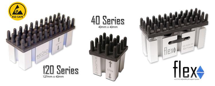
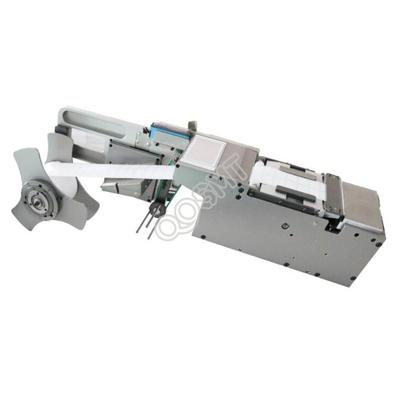
Count On Tools Inc., a leading provider of precision components and SMT spare parts, introduces the new ezLOAD PCB Support System. With the recent increase of densely populated double-sided circuit boards, COT recognized the need for more affordable
Electronics Forum | Fri Nov 27 00:36:02 EST 2015 | slouis2014
I just encountered a BGA design were in, underneath the BGA is a silkscreen that covered the entire bottom of the component except for the copper pads. Can you give any information and advice for this type of design.
Electronics Forum | Fri Dec 20 09:01:27 EST 2002 | russ
Greetings, Does anybody out there have any experience with 0306 capacitors (not 0603). I am trying to find a pad design for this component. I have searched the archives to no avail. The component is .06 long by .03 wide with .007" solder terminat
Used SMT Equipment | In-Circuit Testers
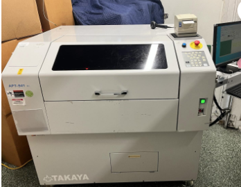
Description Make: Takaya Model: APT-9411CE Year: 2010 Type: Flying Probe Details: Takaya APT 9411 CE Flying Probe The APT-9411CE is designed for users who are looking for a precise and reliable test system with an easy to use softwar
Used SMT Equipment | Board Cleaners
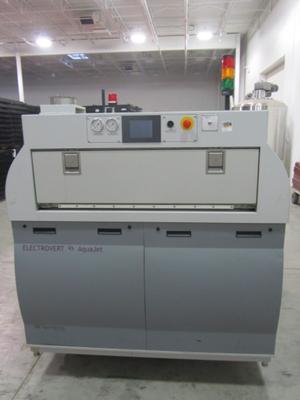
Speedline Technologies AquaJet Stencil Batch Cleaner and Resys ClosedLoop System For Sale The wash needs a control board. (Part Description: BL1700 CNTRL 16IN 16OUT) The Part Number to Purchase this board is 20-101-0214. Estimated cost is $349. We h
Industry News | 2003-06-17 08:07:40.0
The Radiall SMT coupler range now includes the new 14.2 x 5.1mm mini type.
Industry News | 2011-03-31 11:54:23.0
Over the past few years, pad cratering has become a vexing problem in lead-free assemblies, largely attributed to problems with the resin used to make a printed board. To help industry eliminate the defect and, at the same time, cut costs, IPC — Association Connecting Electronics Industries® has released IPC-9708, Test Methods for Characterization of PCB Pad Cratering.
Parts & Supplies | Circuit Board Assembly Products
PULANG TECHNOLOGY CO,.LTDOffers electronic manufacturing services including PCB designing, electronic contract manufacturing including electronic product design, electronic product development, electronic product repair, PCB manufacturing, electronic
Parts & Supplies | Pick and Place/Feeders
Samsung Label feeder Features: • Simple to use. • Automatically places labels using existing pick-and-place machine, Labels are simply treated like any other component. • Not only pastes labels(2D Code ,Barcode, se
Technical Library | 2020-05-08 18:22:31.0
A customer contacted the Helpline to perform analysis on a lead-free assembly which exhibited intermittent functionality. The lead-free assembly exhibiting intermittent functionality when pressure was applied to the ball grid array (BGA) packages. Industrial adaptation of a Restriction of Hazardous Substances (RoHS) compliant solder standard has created a new host of failure modes observed in lead-free assemblies. Pad cratering occurs when fractures propagate along the epoxy resin layer on the underside of the BGA connecting pads. While originating from process, design, and end use conditions, it is the combination of a rigid lead-free solder with inflexible printed circuit board (PCB) laminates that has advanced the prevalence of this condition. Pad cratering is simply the result of mechanical stress exceeding material limitations.
Technical Library | 2019-05-29 01:47:22.0
1.Vias near SMD pads: Solder can flow into the via after melted. As a result cold joint will appear in the end. Check the picture below. 2.Vias on SMD pads: Solder can flow into the via more easier after melted. Check the picture below. 3.Via opening without soldermask covered. When workers solder TH parts by hand, soldering iron can touch vias sometime, then tiny amounts molten solder will stay on vias. This can lead to electrical short easily. We recommend you make all vias tenting (covered by solder mask) if it is possible.
PCBNPI-Professional PCB Fab/PCB Assembly Service Provider From China

www.unisoft-cim.com/pcbtest.htm - In minutes the Unisoft ProntoTEST-FIXTURE software translates CAD & BOM files into real reference designators, netlists, X/Y component pin geometries, values, tolerances, part numbers, etc. This data is used by Test

The PCB Footprint Expert is a powerful CAD library development tool powered by our own proprietary CAD LEAP Technology (Libraries Enhanced with Automated Preferences). It is packed with very powerful advanced library management features that cuts foo
Training Courses | | | PCB Rework and Hand Soldering Courses
The PCB rework and hand soldering courses courses cover techniques of rework and repair of PCBs, BGAs and other electronics assemblies, and teach fundamentals of soldering of electronics assemblies.
Training Courses | | | PCB Rework and Hand Soldering Courses
The PCB rework and hand soldering courses courses cover techniques of rework and repair of PCBs, BGAs and other electronics assemblies, and teach fundamentals of soldering of electronics assemblies.
Events Calendar | Thu Oct 03 00:00:00 EDT 2019 - Thu Oct 03 00:00:00 EDT 2019 | ,
IPC Tech Ed Webinar Series: Ball Grid Array (BGA) and Bottom Termination Component (BTC) Design and Assembly Challenges: Reflow Profiling to Achieve Low Defect Rates and Successful Assembly! – Part 2
Events Calendar | Wed Apr 20 00:00:00 EDT 2022 - Wed Apr 20 00:00:00 EDT 2022 | ,
Virtual Course: Selection Criteria of Surface Finish for Next Generation PCB Technologies
Career Center | Sherman, Texas USA | Engineering,Production,Research and Development,Technical Support
SMT Packaging Engineer: Location: Texas - Sherman , TX Group: HVAL Degree Requirements: BS ME/ChemE/Materials The person in this position will have the ability to make very significant financial contributions to TI because this is a very critic
Career Center | Lincoln, Nebraska USA | Engineering
Brief Description of Job Duties: Provide new program engineering support with emphasis on technical SMT process development. Key activities would include recommendations and implementation of components, SMT pad design, solder methods, testing and r
Career Center | Newport Beach, California USA | Engineering,Management,Production
KEVIN RAGER P.O.BOX 7878, NEWPORT BEACH, 949 922 8997, KEVIN.RAGER@EDA-INC.US OBJECTIVE I am trying to find a consistent work flow that provides mentally challenging yet stimulating experiences in design and prototype development. EXPERIENCE 1997
SMTnet Express, August 13, 2015, Subscribers: 23,186, Members: Companies: 14,558 , Users: 38,745 Pad Cratering Susceptibility Testing with Acoustic Emission Wong Boon San, Julie Silk; Agilent Technologies | Richard Nordstrom, Ph.D.; Acoustic


