Electronics Manufacturing Technical Articles

Electronics Manufacturing Technical Articles

Papers and articles related to SMT, PCB & EMS industry.


  • Reflow Ovens
  • Precision, fluid dispensing systems for low volume, high mix, R&D, and high volume 24x7 production

This article does not exist or has been removed.

Browse other Technical Library articles.

Add Article »

1804 SMT / PCB Assembly Related Technical Articles

SOMABLACK

Jun 28, 2024 | Abby Young

SOMABLACK, produced by Somar Corporation, is rapidly becoming the top choice for many applications that require low to zero light reflectivity. It is a polyester-based material, mixed with black carbon to create something that both shades light and reduces reflection, while also having excellent dimensional stability. It is available in a range of options, with varying thicknesses, specular glossiness, optical density, and coatings....

Publisher: A-Laser, Inc.

A-Laser, Inc.

Custom laser cutting services and precision parts manufacturing.

Milpitas, California, USA

Consultant / Service Provider, Manufacturer

UV Lasers and Kapton

Jun 26, 2024 | A-Laser

How UV lasers cut Kapton and where you can find more information about it....

Publisher: A-Laser, Inc.

A-Laser, Inc.

Custom laser cutting services and precision parts manufacturing.

Milpitas, California, USA

Consultant / Service Provider, Manufacturer

Effects of Flux and Reflow Parameters on Lead-Free Flip Chip Assembly

Jun 23, 2024 | Sandeep Tonapi, Peter Borgesen, Ph.D. K. Srihari, Ph.D

The melting temperatures of most lead-free solder alloys are somewhat higher than that of eutectic Sn/Pb solder, and many of the alloys tend to wet typical contact pads less readily. This tends to narrow down the fluxing and mass reflow process windows for assembly onto typical organic substrates and may enhance requirements on placement accuracy. Flip chip assembly here poses some unique challenges. The small dimensions provide for particular sensitivities to wetting and solder joint collapse, and underfilling does not reduce the demands on the intermetallic bond strength. Rather, the need to underfill lead to additional concerns in terms of underfill process control and reliability. Relatively little can here be learned from work on regular SMT components, BGAs or CSPs....

Publisher: Binghamton University

Binghamton University

Binghamton as an institution is dedicated to higher education, one that combines an international reputation for graduate education, research, scholarship and creative endeavor with the best undergraduate programs available at ...

Binghamton, New York, USA

Research Institute / Laboratory / School

EFFECT OF PROCESS THERMAL HISTORY ON THE MICROSTRUCTURE OF COPPER PILLAR SnAg SOLDER JOINTS

Jun 23, 2024 | Mohammed Genanu, Jim Wilcox , Eric Cotts, Jae Joon Choi, Ki Seok Kim

Two extremes of reflow time scale for copper pillar flip chip solder joints were explored in this study. Sn-2.5Ag solder capped pillars were joined to laminate substrates using either conventional forced convection reflow or the controlled impingement of a defocused infrared laser. The laser reflow joining process was accomplished with an order of magnitude reduction in time above liquidus and a similar increase in solidification cooling rate. The brief reflow time and rapid cooling of a laser impingement reflow necessarily affects all time and temperature dependent phenomena characteristic of reflowed molten solder. These include second phase precipitate dissolution, base metal (copper) dissolution, and the extent of surface wetting. This study examines the reflow dependent microstructural aspects of flip chip Sn-Ag joints on samples of two different size scales, the first with copper pillars of 70μm diameter on 120μm pitch and the second with 23μm diameter pillars on a 40μm pitch. The length scale of Pb-free solder joints is known to affect the Sn grain solidification structure; Sn grain morphology will be noted across both reflow time and joint length scales. Sn grain morphology was further found to be dependent on the extent of surface wetting when such wetting circumvented the copper diffusion barrier layer. Microstructural analysis also will include a comparison of intermetallic structures formed; including the size and number density of second phase Ag3Sn precipitates in the joint and the morphology and thickness of the interfacial intermetallics formed on the pillar and substrate surfaces....

Publisher: Binghamton University

Binghamton University

Binghamton as an institution is dedicated to higher education, one that combines an international reputation for graduate education, research, scholarship and creative endeavor with the best undergraduate programs available at ...

Binghamton, New York, USA

Research Institute / Laboratory / School

Metal Plating Services

Jun 21, 2024 | Abby Young

Explanation of metal plating services and its benefits...

Publisher: A-Laser, Inc.

A-Laser, Inc.

Custom laser cutting services and precision parts manufacturing.

Milpitas, California, USA

Consultant / Service Provider, Manufacturer

Case study: Precise Coating on Electronic Hearing Devices

Jun 20, 2024 | Nordson Electronics Solutions

A leading electronic hearing device manufacturer reduced UV precise coating cycle time by 79% with advanced automation. A manual process of hand brushing UV coating onto components was replaced by an automated solution from Nordson to increase production volumes, improve quality, and reduce costs for this complex application. Download the paper to learn the details of the application....

Publisher: ASYMTEK Products | Nordson Electronics Solutions

ASYMTEK Products | Nordson Electronics Solutions

A leader in automated fluid dispensing, jetting, and conformal coating. Products include stand-alone dispensing workstations and fully automated, in-line conveyorized systems with advanced process controls.

Carlsbad, California, USA

Manufacturer

Component Reliability After Long Term Storage

Jun 19, 2024 | R. R. Madsen

Each year the semiconductor industry routes a significant volume of devices to recycling sites for no reliability or quality rationale beyond the fact that those devices were stored on a warehouse shelf for two years. This study identifies the key risks attributed to extended storage of devices in uncontrolled indoor environments and the risk mitigation required to permit safe shelf-life extension. Component reliability was evaluated after extended storage to assure component solderability, MSL stability and die surface integrity. Packing materials were evaluated for customer use parameters as well as structural integrity and ESD properties. Results show that current packaging material (mold compound and leadframe) is sufficiently robust to protect the active integrated circuits for many decades and permit standard reflow solder assembly beyond 15 years. Standard packing materials (bags, desiccant, and humidity cards) are robust for a 32 month storage period that can be extended by repacking with fresh materials. Packing materials designed for long term storage are effective for more than five years....

Publisher: Texas Instruments

Texas Instruments

Advance in DSP technology and design/applications

Baguio City, USA

Guidelines for the Long-Term Storage of Components, Subasseemblies and Devuces

Jun 19, 2024 | ZVEI-German Electro and Digital Industry Association

These guidelines on long-term storage are intended to help develop a supply strategy for components which need to be warehoused, processed and used beyond ......

Publisher: ZVEI - German Electro and Digital Industry Association

ZVEI - German Electro and Digital Industry Association

The ZVEI is one of the most important manufacturers' associations in Germany. It represents the interests of a high-tech branch with a very widely varied and extremely dynamic product portfolio.

Frankfurt am Main, Germany

Association / Non-Profit

EFFECTS OF STORAGE ENVIRONMENTS ON THE SOLDERABILITY OF NICKELPALLADIUM-GOLD FINISH WITH Pb-BASED AND PbFREE SOLDERS

Jun 19, 2024 | Edwin Lopez, Paul Vianco, Samuel Lucero, and Carly George

The solderability of a nickel-palladium-gold (Ni-Pd-Au) finish on a Cu substrate was evaluated for the Pb-free solder, 95.5Sn-3.9Ag-0.6 Cu (wt.%, abbreviated Sn-Ag-Cu) and the eutectic 63Sn-37 Pb (Sn-Pb) alloy. The solder temperature was 245ºC. The flux was a rosin-based mildly activated (RMA) solution. The Ni-Pd-Au finish was tested in the as-fabricated condition as well as after exposure to one of the following accelerated storage (shelf life) regiments:...

Publisher: Sandia National Laboratories

Sandia National Laboratories

For more than 60 years, Sandia has delivered essential science and technology to resolve the nation's most challenging security issues.

Albuquerque, New Mexico, USA

Other

What Is Laser Engraving

Jun 18, 2024 | A-Laser

An Introduction to laser engraving giving examples of applications....

Publisher: A-Laser, Inc.

A-Laser, Inc.

Custom laser cutting services and precision parts manufacturing.

Milpitas, California, USA

Consultant / Service Provider, Manufacturer

What Is Laser Engraving?

Jun 18, 2024 | A-Laser

An introduction to laser engraving, with applications and why laser engraving is used....

Publisher: A-Laser, Inc.

A-Laser, Inc.

Custom laser cutting services and precision parts manufacturing.

Milpitas, California, USA

Consultant / Service Provider, Manufacturer

High Precision Laser Cutting

Jun 14, 2024 | Abby Young

This type of laser cutting is the most successful and effective practice to achieve quality clean edges and superior products. As opposed to more traditional methods (water jets, punches), laser cutting allows the material to be processed once with extraordinary accuracy and without any other interventions to get a finished piece. It also allows for less waste and is less time consuming, resulting in cleaner production and the ability to manufacture in greater quantities. No matter how complex or straightforward, we achieve the precise, fine cut, details your company needs....

Publisher: A-Laser, Inc.

A-Laser, Inc.

Custom laser cutting services and precision parts manufacturing.

Milpitas, California, USA

Consultant / Service Provider, Manufacturer

What is CNC Laser Cutting For PCB's and other materials

Jun 10, 2024 | A-Laser

A description of CNC laser cutting....

Publisher: A-Laser, Inc.

A-Laser, Inc.

Custom laser cutting services and precision parts manufacturing.

Milpitas, California, USA

Consultant / Service Provider, Manufacturer

What is PCB Depaneling

Jun 07, 2024 | A-Laser

A description of laser PCB Depaneling, the technology used and benefits....

Publisher: A-Laser, Inc.

A-Laser, Inc.

Custom laser cutting services and precision parts manufacturing.

Milpitas, California, USA

Consultant / Service Provider, Manufacturer

What is Laser Routing with Ablation

Jun 07, 2024 | A-Laser

A description of laser routing with ablation....

Publisher: A-Laser, Inc.

A-Laser, Inc.

Custom laser cutting services and precision parts manufacturing.

Milpitas, California, USA

Consultant / Service Provider, Manufacturer

What is Laser Routing with Ablation

Jun 07, 2024 | A-Laser

A description of laser routing with ablation....

Publisher: A-Laser, Inc.

A-Laser, Inc.

Custom laser cutting services and precision parts manufacturing.

Milpitas, California, USA

Consultant / Service Provider, Manufacturer

Gaskets For The Semi Conductor Industry

Jun 05, 2024 | A-Laser

What type of materials are being used for gaskets in the semi-conductor industry....

Publisher: A-Laser, Inc.

A-Laser, Inc.

Custom laser cutting services and precision parts manufacturing.

Milpitas, California, USA

Consultant / Service Provider, Manufacturer

Interesting Materials Used For Gaskets

Jun 04, 2024 | A-Laser

A description of materials called Grafoil and Q-Pad, often used for gaskets....

Publisher: A-Laser, Inc.

A-Laser, Inc.

Custom laser cutting services and precision parts manufacturing.

Milpitas, California, USA

Consultant / Service Provider, Manufacturer

Medical Device Laser Cutting: Applications

Jun 03, 2024 | A-Laser

How Laser cutting can support medical electronics singulation of PCB and for medical components....

Publisher: A-Laser, Inc.

A-Laser, Inc.

Custom laser cutting services and precision parts manufacturing.

Milpitas, California, USA

Consultant / Service Provider, Manufacturer

Precision Aerospace Parts

May 31, 2024 | Abby Young

A-Laser enters the aerospace world with laser cutting services that continue to exceed performance expectations. The modern aerospace industry has strict tolerance requirements and A-Laser is prepared to meet those needs. For example, modern aerospace design dictates anywhere from dozens to millions of precise holes and channels. These must vary in thickness, diameters, and geometries. A-Laser is prepared to meet these requirements and we do so with faster, more versatile, more consistent and cost-effective tools....

Publisher: A-Laser, Inc.

A-Laser, Inc.

Custom laser cutting services and precision parts manufacturing.

Milpitas, California, USA

Consultant / Service Provider, Manufacturer

Achieving Tight Tolerances

May 31, 2024 | Abby Young

A tight tolerance machine isn't necessarily a specific machine type. Rather, it's any machine capable of producing parts with precision tolerances. This means minimal variation in the final dimensions of the part. These cutting-edge tools are meticulously engineered to achieve exceptionally precise measurements within minuscule margins. This is accomplished with CNC, or computer numerical control, a manufacturing method that automates the movement of a machine and optimizes for precision. With technology and advanced techniques, these machines ensure that every component meets exact specifications, guaranteeing unparalleled accuracy in manufacturing processes....

Publisher: A-Laser, Inc.

A-Laser, Inc.

Custom laser cutting services and precision parts manufacturing.

Milpitas, California, USA

Consultant / Service Provider, Manufacturer

Quality Laser Cut Parts

May 31, 2024 | Abby Young

We strive to produce quality parts for customers around the world looking for laser cutting precision. We are able to produce quality machined parts to the specifications provided by customers because of the strong quality system. Precision parts with tight laser cut hole tolerances cannot be done without our quality department. Supplying quality machined parts defines who we are and laser micromachining wouldn't be possible without it....

Publisher: A-Laser, Inc.

A-Laser, Inc.

Custom laser cutting services and precision parts manufacturing.

Milpitas, California, USA

Consultant / Service Provider, Manufacturer

What Is A CNC Machine?

May 30, 2024 | A-Laser

Overview of what a CNC Machine is....

Publisher: A-Laser, Inc.

A-Laser, Inc.

Custom laser cutting services and precision parts manufacturing.

Milpitas, California, USA

Consultant / Service Provider, Manufacturer

What is a CO2 Laser?

May 29, 2024 | A-Laser

An overview of what CO2 laser technology is....

Publisher: A-Laser, Inc.

A-Laser, Inc.

Custom laser cutting services and precision parts manufacturing.

Milpitas, California, USA

Consultant / Service Provider, Manufacturer

Smart Determination of Gold Content in PCBs of Waste Mobile Phones by Coupling of XRF and AAS Techniques

May 28, 2024 | Nicolò Maria Ippolito , Gianmaria Belardi , Valentina Innocenzi , Franco Medici , Loris Pietrelli and Luigi Piga

: Quantitative determination of most economic valuable metals in waste is the first fundamental operation of evaluating the feasibility of recycling processes. Field-portable X-ray fluorescence
spectrometers (FPXRFs) represent a more practical, efficient, and economic tool in determining the
elemental composition of samples with respect to conventional analytical techniques, such as atomic
absorption spectrometry (AAS) and inductively coupled plasma emission spectrometry (ICP). In
this paper, quick and smart determination of gold content in printed circuit boards (PCBs) of waste
mobile phones was studied. The aim of the research was to combine the practicality of FPXRFs
with the reliability of quantitative spectrometry analysis and evaluate the error between the two
techniques. Several samples (33) of PCBs were ground to a size below 0.5 mm, and then, the powders
were analyzed by FPXRFs at different acquisition times with five replications for each sample. The
same analyzed samples then underwent chemical attack to determine the quantitative gold content
by AAS. The obtained results were associated with FPXRFs response with the purpose of realizing
a calibration curve (100–1000 mg/kg Au). The curve was validated for accuracy and precision by
other PCBs waste samples; the control samples were added as standards to obtain a more reliable calibration curve. The curve was evaluated with RPD classification, regression linear, and Bolt–Altman
analysis. 

...

Publisher: University of L'Aquila

University of L'Aquila

The University of L'Aquila is a public research university located in L'Aquila, Central Italy. It was founded in 1964 and is organized in nine departments. The university presents a scientific-technological character with many ...

L'Aquila AQ, Italy

Research Institute / Laboratory / School

Theory of XRF

May 28, 2024 | Peter Brouwer

This booklet gives a general introduction to X-Ray fluorescence (XRF) spectrometry and XRF analysis. It explains simply how a spectrometer works and how XRF analysis is done. It is intended for people new to the field of XRF analysis. Difficult mathematical equations are avoided and the booklet requires only a basic knowledge of mathematics and physics.

The booklet is not dedicated to one specific type of spectrometer or one application area, but aims to give a broad overview of the main spectrometer types and applications.

Chapter 2 briefly explains XRF and its benefits. Chapter 3 explains the physics of XRF, and Chapter 4 describes how this physics is applied to spectrometers and their components. Chapter 5 explains how an XRF analysis is done. It describes the process of sample taking, measuring the sample and calculating the composition from the measurement results.

Finally, Chapter 6 gives a list of recommended literature for further information on XRF analysis.


...

Publisher: Malvern Panalytical Ltd

Malvern Panalytical Ltd

Malvern Panalytical is a Spectris plc company. The company is a manufacturer and supplier of laboratory analytical instruments. It has been influential in the development of the Malvern Correlator, and it remains notable for I...

Malvern, United Kingdom

Manufacturer

Non-Destructive Characterization of Mechanically Processed Waste Printed Circuit Boards: X-ray Fluorescence Spectroscopy and Prompt Gamma Activation Analysis

May 28, 2024 | Akira Otsuki , Pedro Pereira Gonçalves , Christian Stieghorst and Zsolt Révay

This work aimed to characterize the deportment/concentration and liberation/association
of the metals and light elements within mechanically processed waste printed circuit boards (PCBs)
that hold the complex and heterogeneous structure and distribution of different material components.
Waste PCBs passed through a series of mechanical processing (i.e., comminution and sieving) for
metal recovery and were then characterized without further destroying the particles in order to
capture their heterogeneity. The characterizations were performed in a laboratory and large-scale
neutron facility. The results obtained with a portable X-ray fluorescence spectroscopy and prompt
gamma activation analysis were compared and confirmed the good agreement and complementarities
in general. The advantages and disadvantages of the two different methods were identified and
discussed in this paper, in relation to their application to the analysis of mechanically processed
PCB particles. 

...

Publisher: Université de Lorraine

Université de Lorraine

Paul Verlaine University – Metz was a French university, based in Metz. It merged with Nancy-I, Nancy-II, and the INPL forming the University of Lorraine. The merger process started in 2009 with the creation of a "pôles de ...

Metz, France

Research Institute / Laboratory / School

Ultraviolet Laser Technology Overview

May 28, 2024 | A-Laser

Review of UV Laser Technology...

Publisher: A-Laser, Inc.

A-Laser, Inc.

Custom laser cutting services and precision parts manufacturing.

Milpitas, California, USA

Consultant / Service Provider, Manufacturer

INTEGRATED MICRO X-RAY FLUORESCENCE AND CHEMOMETRIC ANALYSIS FOR PRINTED CIRCUIT BOARDS RECYCLING

May 28, 2024 | Silvia Serranti , Giuseppe Capobianco and Giuseppe Bonifazi

A novel approach, based on micro X-ray fluorescence (µXRF), was developed to define an efficient and fast automatic recognition procedure finalized to detect and
topologically assess the presence of the different elements in waste electrical and
electronic equipment (WEEE). More specifically, selected end-of-life (EOL) iPhone
printed circuit boards (PCB) were investigated, whose technological improvement
during time, can dramatically influence the recycling strategies (i.e. presence of
different electronic components, in terms of size, shape, disposition and related
elemental content). The implemented µXRF-based techniques allow to preliminary
set up simple and fast quality control strategies based on the full recognition and
characterization of precious and rare earth elements as detected inside the electronic boards. Furthermore, the proposed approach allows to identify the presence
and the physical-chemical attributes of the other materials (i.e. mainly polymers),
influencing the further physical-mechanical processing steps addressed to realize
a pre-concentration of the valuable elements inside the PCB milled fractions, before
the final chemical recovery

...

Publisher: Sapienza - University of Rome

Sapienza - University of Rome

The Sapienza University of Rome, formally the Università degli Studi di Roma "La Sapienza", abbreviated simply as Sapienza, is a public research university located in Rome, Italy.

Roma RM, Italy

Research Institute / Laboratory / School

Engineering Services

May 23, 2024 | A-Laser

Information on how A-Laser can help support your next laser manufacturing project....

Publisher: A-Laser, Inc.

A-Laser, Inc.

Custom laser cutting services and precision parts manufacturing.

Milpitas, California, USA

Consultant / Service Provider, Manufacturer

Ultraviolet Laser Technology Overview

May 22, 2024 | A-Laser

This article reviews UV or ultraviolet laser technology. Is on method that can be used for laser depaneling or singulation for precision control....

Publisher: A-Laser, Inc.

A-Laser, Inc.

Custom laser cutting services and precision parts manufacturing.

Milpitas, California, USA
Consultant / Service Provider, Manufacturer

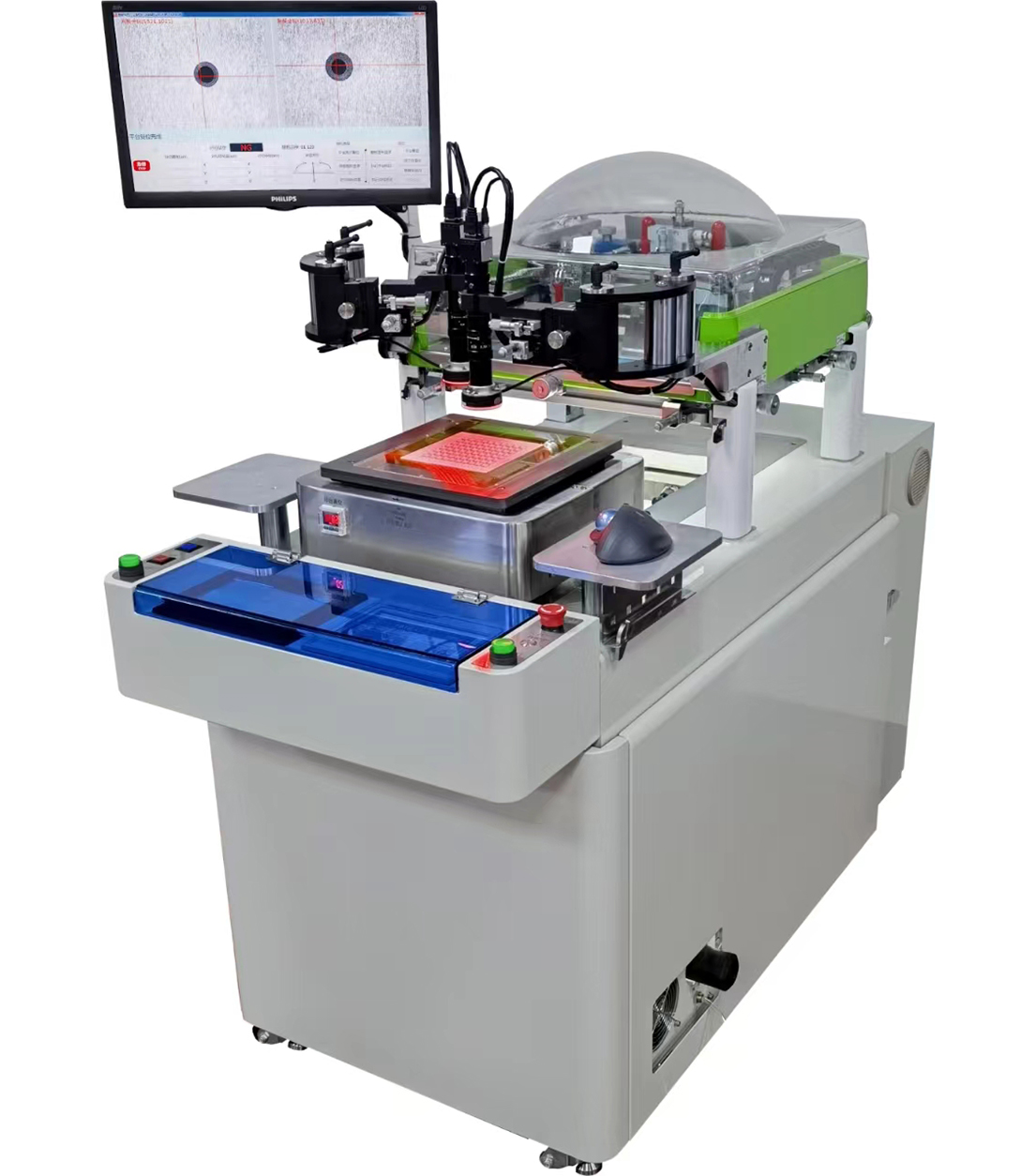
Thick Film Printing Filter , size 6mmx10mm

May 17, 2024 | Max.

Applications: Realize standard thick film printing system, ceramic metallization printing, through hole metallization printing, flexible plate printing such as PET (with micro-hole vacuum printing platform), and solder paste printing of PCB. Features: Ø Automatic screen cleaning function Ø Lighting system:screen lighting, printing table lighting and backlight to check printing effect Ø Can be equipped with conventional center positioning fixture (ceramic substrate thickness >0.38mm) Ø Can be equipped with lifting type center positioning fixture (ceramic substrate >0.1mm) Specifications: Maximum Frame Size: 355x320mm Maximum Printing Area: 150 x 150mm...

Publisher: Wisdom Electronics Co,LTD.

Wisdom Electronics Co,LTD.

Design and manufacturing thick film printing machine for HIC,LTCC,HTCC,chip components,sensors,professional equipment provider,thick film printer,furnace, dryer,laser trimming,thick & thin film technology.

Jiaxing, China

Distributor, Manufacturer

Laser Drilling as an Alternative for Via & Microvia Drilling

May 16, 2024 | A-Laser

Much like actual cities where streets and roads connect buildings together, ICs on a board are connected to each other with copper traces. And just like any metropolitan city, urban expansion tends to move vertically instead of horizontally, but instead of multi-story buildings, we get multilayer boards. Vias are copper-plated holes spanning through the different layers of a given board or panel. They are the entrance locations to the subway stations, if you will. Having those multilayer boards has enabled electronic design to minimize the size of boards immensely without compromising on the complexity....

Publisher: A-Laser, Inc.

A-Laser, Inc.

Custom laser cutting services and precision parts manufacturing.

Milpitas, California, USA

Consultant / Service Provider, Manufacturer

Thick Film Screen Printer J7208

May 14, 2024 | Max.

Applications: High performance sensors, chip elements, thick film circuit (automotive\military\aerospace\medical applications) chip resistance and capacitance, LTCC, HTCC,HIC, RFID (radio frequency identification system) circuit/antenna, high-power LED and other fields. Features: Redefine key variables and standards for high-end printing Dynamic data will change the perception of the printing process Log recording, can trace daily printing data Automatic stabilization and compensation algorithm for printing target film thickness Core patent structure, stable operation period of more than ten years Operator perspective concept, smart using Thirty years of process precipitation, ten years of research and development Three variables affect the stability of film thickness Pressure applied by the squeegee Elasticity of silk screen deformation Pressure on the pad G-level measurement pressure real-time display of three major variables The reaction of the paste scraping rolling will be dynamically displayed Rely on algorithm to achieve uneven correction of front and rear film thickness Screen attenuated scraping wear will be monitored and corrected Ceramic substrate deviation and warping will be monitored and indicated Automatic balance correction can make the screen pattern synchronous recurrence, the uneven phenomenon of film thickness can be eliminated almost can achieve zero pressure printing, ultra-thin easy fragmentation printing will no longer be difficult Specifications: Maximum Frame 450×450mm Maximum Printing area 250×250mm...

Publisher: Wisdom Electronics Co,LTD.

Wisdom Electronics Co,LTD.

Design and manufacturing thick film printing machine for HIC,LTCC,HTCC,chip components,sensors,professional equipment provider,thick film printer,furnace, dryer,laser trimming,thick & thin film technology.

Jiaxing, China

Distributor, Manufacturer

Application of thick film technology- Heaters

May 11, 2024 | Max.

Heaters built on stainless steel substrates have been a popular choice for many applications over the past years because of their high reliability, extended lifetimes, temperature cycling, and power handling capabilities. These characteristics make them a great choice for automotive applications, and this is evident from their current use in the EV space for BMS and cabin comfort. Positive thermal coefficient (PTC) block heaters are the incumbent technology for heating applications in vehicles, however thick film heaters can handle high power density even in the smallest space available, much higher then what you could realize with conventional PTC blocks (stacked in an aluminum gasket). Thick film heaters can also run at much higher temperature than PTCs, as PTCs lose their self-controlling effect when operating at high temperatures or even degrade. Applications: Automotive: electrical vehicle battery thermal management, cabin and comfort heating, heaters for sensors in autos, incl. advanced driver assistance Industrial: food service, white goods, thermal print heads, e-cigarettes Semiconductor: wafer processing Aerospace: instrumentation, sensors Medical: analytical equipment, temperature optimization for sensors...

Publisher: Wisdom Electronics Co,LTD.

Wisdom Electronics Co,LTD.

Design and manufacturing thick film printing machine for HIC,LTCC,HTCC,chip components,sensors,professional equipment provider,thick film printer,furnace, dryer,laser trimming,thick & thin film technology.

Jiaxing, China

Distributor, Manufacturer

Application of thick film technology e-cigarette and heater

May 11, 2024 | Max.

Thick film technology is well established in the automotive industry for high reliability circuitry, challenging sensor applications, and robust passive component needs. With the evolution of electric vehicle (EV) and battery management systems (BMS), the needs for thick film materials are expanding once again. Electronic content per vehicle is doubling and tripling in comparison to current internal combustion engine (ICE) vehicles, and this will expand depending on the level of driving autonomy. One key difference comparing EV to ICE is the waste heat generation. ICE vehicles have utilized this waste heat for several purposes including in-cabin heating. However, EVs must utilize active heating systems, as the waste heat generated from the battery systems is not sufficient to fulfill the needs for cabin comfort. Additionally, battery management systems are required to provide critical temperature control for startup, operation, and charging of the battery pack. This is particularly needed for EV use in colder climates. Thick film is extremely well suited for this application because of the heating precision and repeatability, space constraints, design flexibility, and power handling capabilities of the technology. A heater is very simply a circuit with controlled resistance to output a desired temperature at a given power input. Depending on the choice of materials, thick film heaters can be self-limiting, or they can be designed with high or low temperature coefficient of resistance depending on the control systems desired. And thick film heaters can be built on numerous substrate types compatible to operating temperatures from below zero to upwards of 700°C with nearly unlimited power requirements. Most commonly thick film heaters are built on stainless steel, but there are also material systems available on polymer substrates, glass, oxide and nitride-based ceramics, and aluminum. There are long-running, commercialized uses for each of these types....

Publisher: Wisdom Electronics Co,LTD.

Wisdom Electronics Co,LTD.

Design and manufacturing thick film printing machine for HIC,LTCC,HTCC,chip components,sensors,professional equipment provider,thick film printer,furnace, dryer,laser trimming,thick & thin film technology.

Jiaxing, China

Distributor, Manufacturer

Application of thick film printing on stainless steel surface

May 11, 2024 | Max.

In this research work thick‐film manufacturing technology on stainless steel baseplates was developed. Adequate adhesion of dielectric IP211 to the steel substrate was achieved only by sand blast roughening. Standard PdAg thick‐film conductors were not solderable to IP211. The solution was to have a separate multilayer dielectric under conductors to be soldered. The reliability of soft soldering and gold wire bonding of thick‐film metallisation on stainless steel and other base plate materials was evaluated. The technology developed was applied to manufacturing an intelligent signal node. Present expertise enables the manufacture of thick‐film hybrids on stainless steel base plates. Development of an industrial production line would, however, involve considerable effort.p J7208 Perfect solution to the printing process...

Publisher: Wisdom Electronics Co,LTD.

Wisdom Electronics Co,LTD.

Design and manufacturing thick film printing machine for HIC,LTCC,HTCC,chip components,sensors,professional equipment provider,thick film printer,furnace, dryer,laser trimming,thick & thin film technology.

Jiaxing, China

Distributor, Manufacturer

Ceramic Substrate Thick Film Screen Printing

May 11, 2024 | Max.

Perfect solution to the problem of uneven printing film thickness caused by poor flatness of ceramic substrate...

Publisher: Wisdom Electronics Co,LTD.

Wisdom Electronics Co,LTD.

Design and manufacturing thick film printing machine for HIC,LTCC,HTCC,chip components,sensors,professional equipment provider,thick film printer,furnace, dryer,laser trimming,thick & thin film technology.

Jiaxing, China

Distributor, Manufacturer

Ceramic Substrate Thick Film Screen Printing

May 11, 2024 | Max.

Perfect solution to the problem of uneven printing film thickness caused by poor flatness of ceramic substrate...

Publisher: Wisdom Electronics Co,LTD.

Wisdom Electronics Co,LTD.

Design and manufacturing thick film printing machine for HIC,LTCC,HTCC,chip components,sensors,professional equipment provider,thick film printer,furnace, dryer,laser trimming,thick & thin film technology.

Jiaxing, China

Distributor, Manufacturer

Thick Film Screen Printer J7212

May 11, 2024 | Max.

High performance sensors, chip elements, thick film circuit (automotive\military\aerospace\medical applications) chip resistance and capacitance, LTCC, HTCC,HIC, RFID (radio frequency identification system) circuit/antenna, high-power LED and other fields. Maximum Frame 750×750mm Maximum printed area 350×350mm...

Publisher: Wisdom Electronics Co,LTD.

Wisdom Electronics Co,LTD.

Design and manufacturing thick film printing machine for HIC,LTCC,HTCC,chip components,sensors,professional equipment provider,thick film printer,furnace, dryer,laser trimming,thick & thin film technology.

Jiaxing, China

Distributor, Manufacturer

Thick Film Screen Printer J7208

May 11, 2024 | Max.

High performance sensors, chip elements, thick film circuit (automotive\military\aerospace\medical applications) chip resistance and capacitance, LTCC, HTCC,HIC, RFID (radio frequency identification system) circuit/antenna, high-power LED and other fields. Maximum Frame 450×450mm Maximum Printing area 250×250mm...

Publisher: Wisdom Electronics Co,LTD.

Wisdom Electronics Co,LTD.

Design and manufacturing thick film printing machine for HIC,LTCC,HTCC,chip components,sensors,professional equipment provider,thick film printer,furnace, dryer,laser trimming,thick & thin film technology.

Jiaxing, China

Distributor, Manufacturer

Thick Film Screen Printer 5206-CX

May 11, 2024 | Max.

Applications: Realize standard thick film printing system, ceramic metallization printing, through hole metallization printing, flexible plate printing such as PET (with micro-hole vacuum printing platform), and solder paste printing of PCB. Features: Automatic screen cleaning function Lighting system:screen lighting, printing table lighting and backlight to check printing effect Can be equipped with conventional center positioning fixture (ceramic substrate thickness >0.38mm) Can be equipped with lifting type center positioning fixture (ceramic substrate >0.1mm) Specifications: Maximum Frame Size: 355x320mm Maximum Printing Area: 150 x 150mm...

Publisher: Wisdom Electronics Co,LTD.

Wisdom Electronics Co,LTD.

Design and manufacturing thick film printing machine for HIC,LTCC,HTCC,chip components,sensors,professional equipment provider,thick film printer,furnace, dryer,laser trimming,thick & thin film technology.

Jiaxing, China

Distributor, Manufacturer

Thick Film Screen Printer J3202B

May 11, 2024 | Max.

Thick film circuit, suitable for thick film printing of heavy workpieces Printing Product Size: 20-70mm...

Publisher: Wisdom Electronics Co,LTD.

Wisdom Electronics Co,LTD.

Design and manufacturing thick film printing machine for HIC,LTCC,HTCC,chip components,sensors,professional equipment provider,thick film printer,furnace, dryer,laser trimming,thick & thin film technology.

Jiaxing, China

Distributor, Manufacturer

Thick Film Screen Printer J3202

May 11, 2024 | Max.

Thick film circuit, pressure sensor (piezoresistive, capacitive), glass glaze potentiometer, dielectric antenna, ceramic metallization RFID, automotive oil level sensor, LED ceramic bracket, tension sensor, piezoelectric ceramic components, etc. Maximum Printing Area: 75x70mm...

Publisher: Wisdom Electronics Co,LTD.

Wisdom Electronics Co,LTD.

Design and manufacturing thick film printing machine for HIC,LTCC,HTCC,chip components,sensors,professional equipment provider,thick film printer,furnace, dryer,laser trimming,thick & thin film technology.

Jiaxing, China

Distributor, Manufacturer

Thick Film Screen Printer J3201

May 11, 2024 | Max.

Applications: Thick film circuit, pressure sensor (Piezoresistive , Capacitive), RF device, ceramic metallization RFID, piezoelectric ceramic components, etc. Most suitable for automatic printing of small and shaped work pieces. Specifications: Printing Area: Diameter 1-25mm,height less than 23mm...

Publisher: Wisdom Electronics Co,LTD.

Wisdom Electronics Co,LTD.

Design and manufacturing thick film printing machine for HIC,LTCC,HTCC,chip components,sensors,professional equipment provider,thick film printer,furnace, dryer,laser trimming,thick & thin film technology.

Jiaxing, China

Distributor, Manufacturer

Thick Film Screen Printer J1202-RS

May 11, 2024 | Max.

Applications: Thick film circuit, pressure sensor (piezoresistive, capacitive), glass glaze potentiometer, dielectric antenna, ceramic metallization, microwave magnetron,HTCC,LTCC,HIC,RFID, automotive oil level sensor, air quality sensor, integrated LED lamp holder, tension sensor, piezoelectric ceramic components, etc Maximum Frame Size: 185x252mm Maximum Printing Area: 70x75mm...

Publisher: Wisdom Electronics Co,LTD.

Wisdom Electronics Co,LTD.

Design and manufacturing thick film printing machine for HIC,LTCC,HTCC,chip components,sensors,professional equipment provider,thick film printer,furnace, dryer,laser trimming,thick & thin film technology.

Jiaxing, China

Distributor, Manufacturer

What is Laser Depaneling/Singulation?

May 10, 2024 | A-Laser

A Review of laser singulation and what it is and how it can benefit PCB Contract Assembly....

Publisher: A-Laser, Inc.

A-Laser, Inc.

Custom laser cutting services and precision parts manufacturing.

Milpitas, California, USA

Consultant / Service Provider, Manufacturer

A review on Automatic Bare PCB Board Testing

May 08, 2024 | S.Kanimozhi, Dr. K.Gopala Krishnan

A Printed Circuit Board is used to mechanically support and electrically connect electronic components using conductive pathways, track or signal traces etched from copper sheets laminated on to anon conductive substrate. The automatic inspection of PCBs serves a purpose which is traditional in computer technology. The purpose is to relieve human inspectors of the tedious and inefficient task of looking for those defects in PCBs which could lead to electric failure. This paper is a survey conducted on various existing approaches which performs automatic testing on PCB.

...

Publisher: Sri Ramakrishna College of Arts & Science

Sri Ramakrishna College of Arts & Science

Sri Ramakrishna College of Arts and Science is a College of Arts and Science in Coimbatore, Tamil Nadu, India. It was founded in 1987. At present, with 5000+ students, the college is offering 30+ programmes in Arts, Humanities ...

Peelamedu, India

Research Institute / Laboratory / School

A Machine Vision Based Automatic Optical Inspection System for Measuring Drilling Quality of Printed Circuit Boards

Apr 29, 2024 | Wei-Chien Wang, Liang-Bi Chen,Wan-Jung Chang, Shang-Liang Chen, and Katherine Shu-Min Li

In this paper, we develop and put into practice an Automatic Optical Inspection (AOI) system based on machine vision to check the holes on a printed circuit board (PCB). We incorporate the hardware and software. For the hardware part, we combine a PC, the three-axis positioning system, a lighting device and CCD cameras. For the software part, we utilize image registration, image segmentation, drill numbering, drill contrast, and defect displays to achieve this system. Results indicated that an accuracy of 5µm could be achieved in errors of the PCB holes allowing comparisons to be made. This is significant in inspecting the missing, the multi-hole and the incorrect location of the holes. However, previous work only focusses on one or other feature of the holes. Our research is able to assess multiple features: missing holes, incorrectly located holes and excessive holes. Equally, our results could be displayed as a bar chart and target plot. This has not been achieved before. These displays help users analyze the causes of errors and immediately correct the problems. Additionally, this AOI system is valuable for checking a large number of holes and finding out the defective ones on a PCB. Meanwhile, we apply a 0.1mm image resolution which is better than others used in industry. We set a detecting standard based on 2mm diameter of circles to diagnose the quality of the holes within 10 seconds....

Publisher: National Cheng Kung University

National Cheng Kung University

National Cheng Kung University is a public research university located in Tainan, Taiwan. NCKU is one of the best comprehensive universities in Taiwan and a leader in promoting industry-academia cooperation. ...

Tainan City, Taiwan

Research Institute / Laboratory / School

FICS-PCB: A Multi-Modal Image Dataset for Automated Printed Circuit Board Visual Inspection

Apr 29, 2024 | Hangwei Lu , Dhwani Mehta, Olivia Paradis, Navid Asadizanjani, Mark Tehranipoor, and Damon L. Woodard

Over the years, computer vision and machine learning disciplines have considerably advanced the field of automated visual inspection for Printed Circuit Board (PCB-AVI) assurance. However, in practice, the capabilities and limitations of these advancements remain unknown because there are few publicly accessible datasets for PCB visual inspection and even fewer that contain images that simulate realistic application scenarios. To address this need, we propose a publicly available dataset, "FICS-PCB"1, to facilitate the development of robust methods for PCB-AVI. The proposed dataset includes challenging cases from three variable aspects: illumination, image scale, and image sensor. This dataset consists of 9,912 images of 31 PCB samples and contains 77,347 annotated components. This paper reviews the existing datasets and methodologies used for PCBAVI, discusses challenges, describes the proposed dataset, and presents baseline performances using feature engineering and deep learning methods for PCB component classification....

Publisher: University of Florida

University of Florida

SVS 8100 (parts)

Gainesville, Florida, USA

Manufacturer

per page.

Pages: 1 2 3 4 5 6 7 8 9 10 11 12 13 14 15 16 17 18 19 20 21 22 23 24 25 26 27 28 29 30 31 32 33 34 35 36 37

Capillary Underfill Dispensing

Software for SMT