Carlos Tafoya, Gustavo Ramirez, Timothy O'Neill; AIM Solder
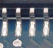
Bottom terminated components, or BTCs, have been rapidly incorporated into PCB designs because of their low cost, small footprint and overall reliability. The combination of leadless terminations with underside ground/thermal pads have presented a multitude of challenges to PCB assemblers, including tilting, poor solder fillet formation, difficult inspection and ��� most notably ��� center pad voiding. Voids in large SMT solder joints can be difficult to predict and control due to the variety of input variables that can influence their formation. Solder paste chemistries, PCB final finishes, and reflow profiles and atmospheres have all been scrutinized, and their effects well documented. Additionally, many of the published center pad voiding studies have focused on optimizing center pad footprint and stencil aperture designs. This study focuses on I/O pad stencil modifications rather than center pad modifications. It shows a no-cost, easily implemented I/O design guideline that can be deployed to consistently and repeatedly reduce void formation on BTC-style packages.
SMTA - Surface Mount Technology Association is a non-profit international association of companies and individuals (totalling 4,000) involved in all aspects of advanced electronics assembly, surface mount and related technologies.
IPC - Association Connecting Electronics Industries is a US-based trade association dedicated to the competitive excellence and financial success of its nearly 2,600 member companies which represent all facets of the electronic interconnection industry, including design, printed wiring board manufacturing and electronics assembly.